Publication
Metrics
AI Quick Summary
This paper demonstrates the fabrication of 3D-printed terahertz topological waveguides using a cost-effective method combining 3D-printing and gold-sputtering, showing a significant improvement in topological bandgap size and robust THz propagation around defects. This offers a promising solution for compact integrated terahertz devices in wireless communications.
Paper Preview
Abstract
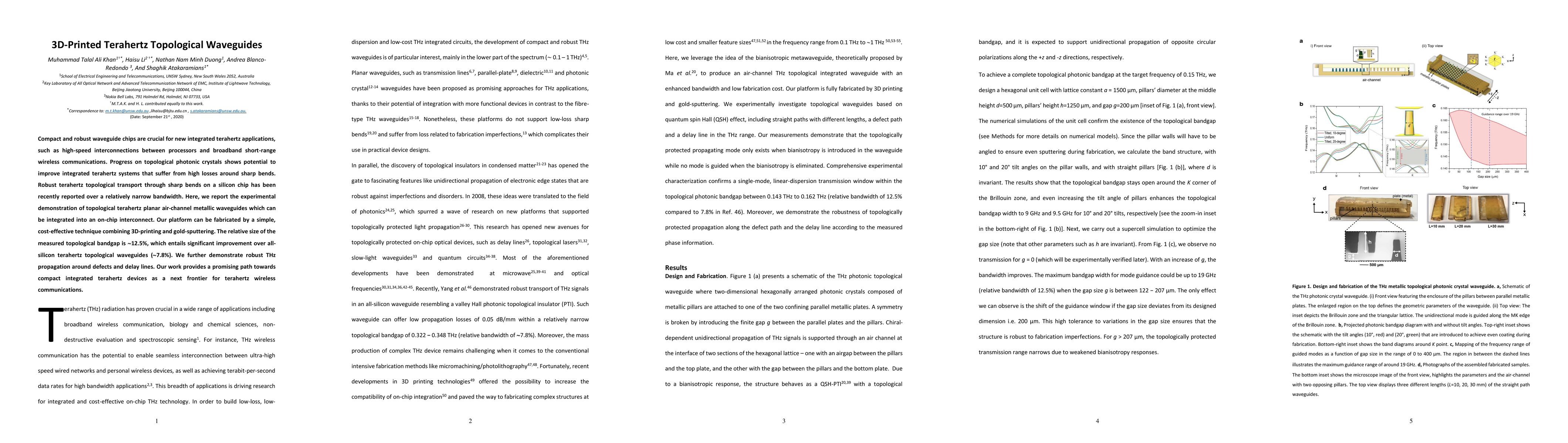
Compact and robust waveguide chips are crucial for new integrated terahertz applications, such as high-speed interconnections between processors and broadband short-range wireless communications. Progress on topological photonic crystals shows potential to improve integrated terahertz systems that suffer from high losses around sharp bends. Robust terahertz topological transport through sharp bends on a silicon chip has been recently reported over a relatively narrow bandwidth. Here, we report the experimental demonstration of topological terahertz planar air-channel metallic waveguides which can be integrated into an on-chip interconnect. Our platform can be fabricated by a simple, cost-effective technique combining 3D-printing and gold-sputtering. The relative size of the measured topological bandgap is ~12.5%, which entails significant improvement over all-silicon terahertz topological waveguides (~7.8%). We further demonstrate robust THz propagation around defects and delay lines. Our work provides a promising path towards compact integrated terahertz devices as a next frontier for terahertz wireless communications.
AI Key Findings
Get AI-generated insights about this paper's methodology, results, significance, and more — seven facets brought into focus.
Impact
Paper Details
Authors
PDF Preview
Key Terms
Citation Network
Current paper (gray), citations (green), references (blue)
Display is limited for performance on very large graphs.
Discussion 0