A Backside-Illuminated Charge-Focusing Silicon SPAD with Enhanced Near-Infrared Sensitivity
Publication
Metrics
AI Quick Summary
This paper presents a backside-illuminated silicon SPAD with enhanced near-infrared sensitivity, featuring a charge-focusing electric field and a 2 μm multiplication region for efficient electron collection. The SPAD achieves a photon detection efficiency of 27% at 905 nm and a timing resolution of 240 ps, suitable for time-of-flight imaging applications.
Paper Preview
Abstract
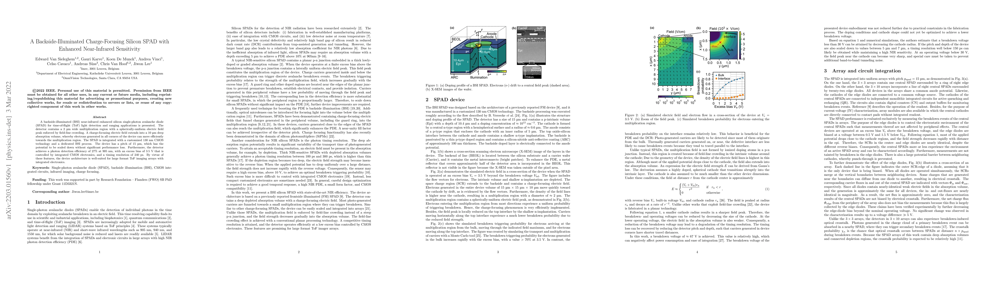
A backside-illuminated (BSI) near-infrared enhanced silicon single-photon avalanche diode (SPAD) for time-of-flight (ToF) light detection and ranging applications is presented. The detector contains a 2 $\mu$m wide multiplication region with a spherically-uniform electric field peak enforced by field-line crowding. A charge-focusing electric field extends into a 10 $\mu$m deep absorption volume, whereby electrons generated in all corners of the device can move efficiently towards the multiplication region. The SPAD is integrated with a customized 130 nm CMOS technology and a dedicated BSI process. The device has a pitch of 15 $\mu$m, which has the potential to be scaled down without significant performance loss. Furthermore, the detector achieves a photon detection efficiency of 27% at 905 nm, with an excess bias of 3.5 V that is controlled by integrated CMOS electronics, and a timing resolution of 240 ps. By virtue of these features, the device architecture is well-suited for large format ToF imaging arrays with integrated electronics.
AI Key Findings
Get AI-generated insights about this paper's methodology, results, significance, and more — seven facets brought into focus.
Impact
Paper Details
Authors
PDF Preview
Key Terms
Citation Network
Current paper (gray), citations (green), references (blue)
Display is limited for performance on very large graphs.
Discussion 0