A Ballistic Two-Dimensional Lateral Heterojunction Bipolar Transistor
Publication
Metrics
AI Quick Summary
This research proposes a novel monolayer ballistic lateral heterojunction bipolar transistor using transition metal dichalcogenides, demonstrating intrinsic thinness and high current modulation ratio of 10$^8$ without the need for gates. Simulations confirm its operational principle, current gain, and potential for THz frequency applications.
Paper Preview
Abstract
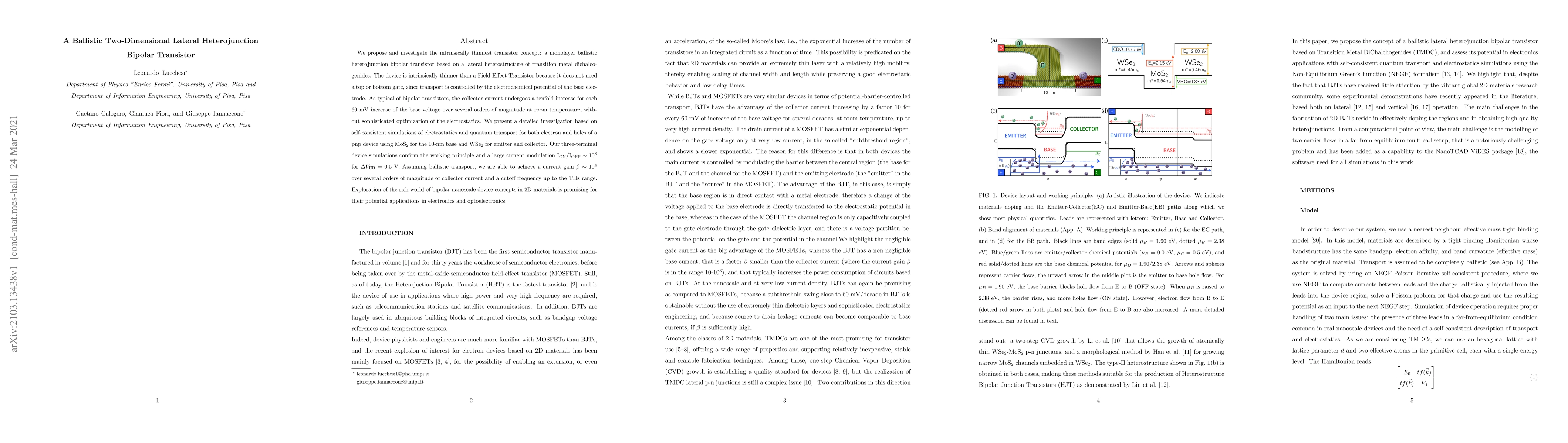
We propose and investigate the intrinsically thinnest transistor concept: a monolayer ballistic heterojunction bipolar transistor based on a lateral heterostructure of transition metal dichalcogenides. The device is intrinsically thinner than a Field Effect Transistor because it does not need a top or bottom gate, since transport is controlled by the electrochemical potential of the base electrode. As typical of bipolar transistors, the collector current undergoes a tenfold increase for each 60 mV increase of the base voltage over several orders of magnitude at room temperature, without sophisticated optimization of the electrostatics. We present a detailed investigation based on self-consistent simulations of electrostatics and quantum transport for both electron and holes of a pnp device using MoS$_2$ for the 10-nm base and WSe$_2$ for emitter and collector. Our three-terminal device simulations confirm the working principle and a large current modulation I$_\text{ON}$/I$_\text{OFF}\sim 10^8$ for $\Delta V_{\rm EB}=0.5$ V. Assuming ballistic transport, we are able to achieve a current gain $\beta\sim$ 10$^4$ over several orders of magnitude of collector current and a cutoff frequency up to the THz range. Exploration of the rich world of bipolar nanoscale device concepts in 2D materials is promising for their potential applications in electronics and optoelectronics.
AI Key Findings
Get AI-generated insights about this paper's methodology, results, significance, and more — seven facets brought into focus.
Impact
Paper Details
Authors
PDF Preview
Key Terms
Citation Network
Current paper (gray), citations (green), references (blue)
Display is limited for performance on very large graphs.
Discussion 0