Quick Summary:

This study compares CVD-grown and mechanically exfoliated MoS$_2$ using optical spectroscopy, revealing differences in phonon modes and strong room-temperature photoluminescence in CVD films, along with significant spectral shifts and valley polarization in PL measurements.

Summary

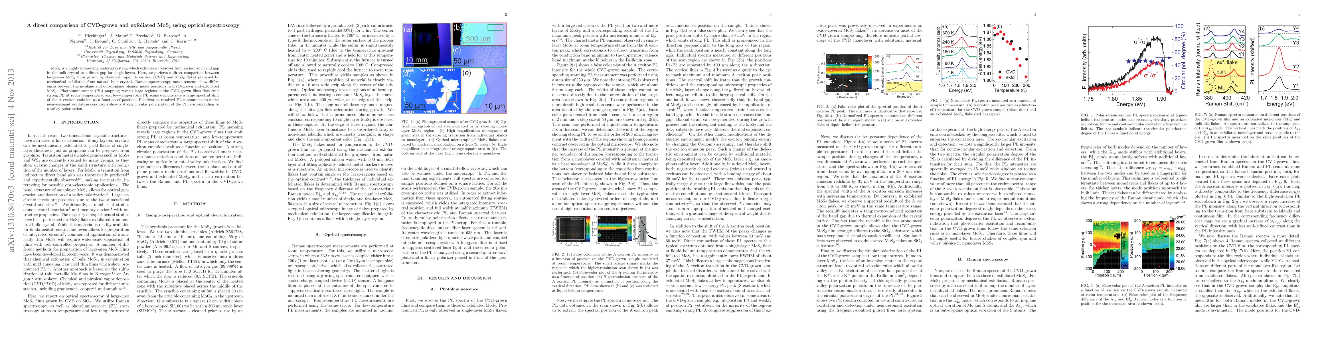
MoS2 is a highly interesting material system, which exhibits a crossover from an indirect band gap in the bulk crystal to a direct gap for single layers. Here, we perform a direct comparison between large-area MoS$_2$ films grown by chemical vapor deposition (CVD) and MoS$_2$ flakes prepared by mechanical exfoliation from natural bulk crystal. Raman spectroscopy measurements show differences between the in-plane and out-of-plane phonon mode positions in CVD-grown and exfoliated MoS$_2$. Photoluminescence (PL) mapping reveals large regions in the CVD-grown films that emit strong PL at room temperature, and low-temperature PL scans demonstrate a large spectral shift of the A exciton emission as a function of position. Polarization-resolved PL measurements under near-resonant excitation conditions show a strong circular polarization of the PL, corresponding to a valley polarization.

AI Key Findings

Get AI-generated insights about this paper's methodology, results, and significance.

Paper Details

PDF Preview

Download PDF

Key Terms

pl (0.379)
_2 (0.238)
polarization (0.218)
films (0.201)
crystal (0.186)
bulk (0.174)
plane (0.156)
direct (0.152)
gap (0.152)
valley (0.145)
exciton (0.145)
band gap (0.140)
raman (0.138)
measurements (0.136)
room temperature (0.134)
crossover (0.133)
indirect (0.133)
prepared (0.131)
strong (0.130)
room (0.129)
Title Authors Year Actions
Asymmetric charge distribution boosts hydrogen evolution performance in two‐dimensional MoO2/MoS2 step heterostructure
Mengke Kang, Xiang Zhang, Jingyi Wang, Wen Li, Tianyu Xue, K. Zhai, J. Xiang, Anmin Nie, Yingchun Cheng, Zhongyuan Liu
2025
View Paper
Unveiling the unexpected sinking and embedding dynamics of surface supported Mo/S clusters on 2D MoS2 with active machine learning
Luneng Zhao, Yanhan Ren, Xiaoran Shi, Hongsheng Liu, Zhigen Yu, Junfeng Gao, Jijun Zhao
2024
View Paper
Atomic vs. sub-atomic layer deposition: impact of growth rate on the optical and structural properties of MoS2 and WS2
C. Tessarek, T. Grieb, F. Krause, Christian Petersen, A. Karg, Alexander Hinz, Niels Osterloh, Christian Habben, Stephan Figge, Jon-Olaf Krisponeit, Thomas Schmidt, Jens Falta, A. Rosenauer, M. Eickhoff
2024
View Paper
Rapid and large-scale synthesis of MoS2 via ultraviolet laser-assisted technology for photodetector applications
T. Xu, Xiangbin Zeng, Shijiao Hu, Wenzhao Wang, Xiaoqing Bao, Yu Peng, Huaicheng Deng, Zhuocheng Gan, Zhiqi Wen, Wenhao Zhang, Lihong Chen
2024
View Paper
Novel Nano-Electroplating-Based Plasmonic Platform for Giant Emission Enhancement in Monolayer Semiconductors.
A. Anand V S, M. K. Sahoo, Faiha Mujeeb, Abin Varghese, Subhabrata Dhar, S. Lodha, Anshuman Kumar
2023
View Paper
Optimization of Layer Transfer and Photolithography for Device Integration of 2D-TMDC
A. Ghiami, Tianyishan Sun, Hleb Fiadziushkin, Songyao Tang, A. Grundmann, M. Heuken, H. Kalisch, A. Vescan
2023
View Paper
Different healing characteristics of thiol-bearing molecules on CVD-grown MoS2
Giovanna Feraco, O. D. Luca, Ali Syari’ati, Sardar Hameed, A. A. El Yumin, Jianting Ye, R. Agostino, P. Rudolf
2023
View Paper
Temperature dependence Raman spectroscopy studies of CVD grown few layer MoS2 triangular domains
S. Rawat, P. Bamola, Monika Bisht, Bhuvan Singh Bhandari, C. Dwivedi, Himani Sharma
2023
View Paper
Advanced development of grain boundaries in TMDs from fundamentals to hydrogen evolution application
Ziyang Yin, Lingbin Xie, Weinan Yin, Ting Zhi, Kang Chen, Junan Pan, Yingbo Zhang, Jingwen Li, Longlu Wang
2023
View Paper
Improved characteristics of MoS2 transistors with selective doping using 1,2-dichloroethane
W. Jeong, Taeyoung Kim, Yoonsok Kim, M. Jeong, Eun Kyu Kim
2023
View Paper
Single step growth of vertical MoS_2 thin films by chemical vapor deposition for hydrogen evolution reaction
S. Saseendran, Anamika Ashok, M. Jayaraj, R. Reshmi, A. Asha
2023
View Paper
Dipole doping effect in MoS2 field effect transistors based on phase transition of ferroelectric polymer dopant
D. Lee, Tae-Kwang Park, Taeho Jeong, Youngkyun Jung, J. Park, Nackyong Joo, U. Won, Hocheon Yoo
2023
View Paper
Efficient Multiple Exciton Generation in Monolayer MoS2.
Ashish Soni, D. Kushavah, Li‐Syuan Lu, Wen‐Hao Chang, S. Pal
2022
View Paper
Size and shape control of CVD-grown monolayer MoS2
Yong-Jin Cho, Yumin Sim, Je-ho Lee, Nguyen The Hoang, M. Seong
2022
View Paper
Effects of CVD growth parameters on global and local optical properties of MoS2 monolayers
Ana Senkić, J. Bajo, A. Supina, B. Radatović, N. Vujičić
2022
View Paper
Analysis of Schottky barrier heights and reduced Fermi-level pinning in monolayer CVD-grown MoS2 field-effect-transistors
Jing Xie, N. Patoary, Guantong Zhou, Mohammed Sayyad, S. Tongay, I. Esqueda
2022
View Paper
Gate-controlled sensing of ammonia by single-layer MoS2 field-effect transistor
N. S. Struchkov, Nikita P. Nekrasov, Aleksei V. Emelianov, Feruza F. Tuyakova, I. Bobrinetskiy
2022
View Paper
Optical Harmonic Generation in 2D Materials
A. Khan, Linglong Zhang, Kashif Ishfaq, A. Ikram, Tanju Yildrim, Boqing Liu, Sharidya Rahman, Yuerui Lu
2021
View Paper
Performances enhancement of graphene/n-Si Schottky junction solar cells with dual-functional MoS2 interfacial layers
Jun Ma, Yujie Yuan, P. Sun
2021
View Paper
Spatiotemporal dynamics of free and bound excitons in CVD-grown MoS2 monolayer
M. A. Akmaev, M. Glazov, M. Kochiev, P. Vinokurov, S. Smagulova, V. Belykh
2021
View Paper
Synthesis of nanosized ultrathin MoS2 on montmorillonite nanosheets by CVD method
Jiexian Zhang, Tianyu Liu, Liangjie Fu, Gonglan Ye
2021
View Paper
Realization of low-power and high mobility thin film transistors based on MoS2 layers grown by PLD technique
Sujit Kumar, Anjali Sharma, M. Tomar, Vinay Gupta
2021
View Paper
In‐Plane and Out‐of‐Plane Optical Properties of Monolayer, Few‐Layer, and Thin‐Film MoS 2 from 190 to 1700 nm and Their Application in Photonic Device Design
Kazi M. Islam, R. Synowicki, Timothy Ismael, Isaac O Oguntoye, Nathan J. Grinalds, M. Escarra
2021
View Paper
Integrated contact lens sensor system based on multifunctional ultrathin MoS2 transistors
Shiqi Guo, Kaijin Wu, Chengpan Li, Hao Wang, Zheng Sun, Dawei Xi, S. Zhang, W. Ding, M. Zaghloul, Changning Wang, F. Castro, Dong Yang, Yunlong Zhao
2020
View Paper
Enhancement of van der Waals interlayer coupling through polar Janus MoSSe.
Kunyan Zhang, Yunfan Guo, Qingqing Ji, Ang-Yu Lu, C. Su, Hua Wang, A. Puretzky, D. Geohegan, Xiaofeng Qian, S. Fang, E. Kaxiras, J. Kong, Shengxi Huang
2020
View Paper
High-performance flexible nanoscale transistors based on transition metal dichalcogenides
A. Daus, S. Vaziri, Victoria Chen, Ç. Köroğlu, R. Grady, C. Bailey, H. Lee, K. Schauble, K. Brenner, E. Pop
2020
View Paper
Coverage-dependent differential reflectance spectra of MoS2 atomic films synthesized by CVD using a large-diameter quartz tube
Yina Wang, Lei Zhang, Hang Xiao, Chenhui Su, Shanshan Lv, Faye Zhang, Q. Sui, L. Jia, Mingshun Jiang
2020
View Paper
Temperature-dependent photoluminescence and time-resolved photoluminescence study of monolayer molybdenum disulfide
H. Li, X. H. Zhang
2020
View Paper
Nanotribological Effect of Water Layers Intercalated between Exfoliated MoS2 and Mica
Dooho Lee, Hyunhwa Lee, Hyunsoo Lee, Jeong Y. Park
2020
View Paper
Facile integration of MoS2/SiC photodetector by direct chemical vapor deposition
Yifan Xiao, Long Min, Xinke Liu, Wenjun Liu, U. Younis, T. Peng, X. Kang, Xiaohan Wu, S. Ding, David-Wei Zhang
2020
View Paper
High output voltage generation of over 5 V from liquid motion on single-layer MoS2
A. Aji, Ryohei Nishi, H. Ago, Y. Ohno
2020
View Paper
Synthesis of High-Quality Monolayer MoS2 by Direct Liquid Injection.
K. McCreary, E. Cobas, A. Hanbicki, M. Rosenberger, Hsun-Jen Chuang, S. Sivaram, V. Oleshko, B. Jonker
2020
View Paper
Anisotropic electron–photon–phonon coupling in layered MoS2
Deepu Kumar, Birender Singh, Rahul Kumar, Mahesh Kumar, Pradeep Kumar
2020
View Paper
High optical quality of MoS2 monolayers grown by chemical vapor deposition
S. Shree, A. George, T. Lehnert, C. Neumann, M. Benelajla, C. Robert, X. Marie, Kenji Watanabe, T. Taniguchi, U. Kaiser, B. Urbaszek, A. Turchanin
2019
View Paper
Paper-Cut Flexible Multifunctional Electronics Using MoS2 Nanosheet
Dong Yang, Hao Wang, Shenglin Luo, Changning Wang, S. Zhang, Shiqi Guo
2019
View Paper
Photoresponse of Optical Sensors Based on Transition Metal Dichalcogenides: Influence of Thickness on Spectral Characteristics
A. Avdizhiyan, S. Lavrov, A. Kudryavtsev, A. Shestakova, M. Vasina
2019
View Paper
Synthesis of Transition Metal Disulfides with Liquid Ammonium Sulfide as a Reliable Sulfur Precursor
Soo Ho Choi, C. Oh, Stephen Boandoh, Woochul Yang, S. Kim, Ki Kang Kim
2019
View Paper
Growth of MoS2 nanoflakes near/far from tubular furnace axis and their impact on the efficiency enhancement of the Si solar cells
Maryam Alsadat Nikpay, S. Z. Mortazavi, A. Reyhani, S. Elahi, A. Taherkhani
2019
View Paper
Effect of nanosecond and femtosecond pulse laser on the formation of WS2 nanostructures and field emission characteristics
P. Koinkar, K. Sasaki, A. Furube, K. Murai, T. Moriga, M. Shinde, S. Rane, S. Bhopale, M. More
2019
View Paper
Probing the Optical Properties of MoS2 on SiO2/Si and Sapphire Substrates
Tao Han, Hongxia Liu, Shulong Wang, Shupeng Chen, Wei Li, Xiaoli Yang, M. Cai, Kun Yang
2019
View Paper
Probing the Growth Improvement of Large-Size High Quality Monolayer MoS2 by APCVD
Tao Han, Hongxia Liu, Shulong Wang, Shupeng Chen, Wei Li, Xiaoli Yang
2019
View Paper
Efficient defect healing of transition metal dichalcogenides by phthalocyanines
Hyeyoung Ahn, Guan-Hua Lee
2019
View Paper
Optical thickness identification of few-layer MoS2 deposited by chemical vapor deposition
Zusong Zhu, D. Zhu, Jie Zhang, Guisheng Jiang, Mingfang Yi, Jun Wen
2019
View Paper
Research on the Factors Affecting the Growth of Large-Size Monolayer MoS2 by APCVD
Tao Han, Hongxia Liu, Shulong Wang, Wei Li, Shupeng Chen, Xiaoli Yang, M. Cai
2018
View Paper
Friction characteristics of mechanically exfoliated and CVD-grown single-layer MoS2
Dinh Le Cao Ky, Bien-Cuong Tran Khac, C. Le, Yong Soo Kim, K. Chung
2018
View Paper
Optical Characterization of the Structural Imperfection of Two-Dimensional MoS2 Crystallites
S. Lavrov, A. Shestakova, A. Avdizhiyan, E. Mishina
2018
View Paper
Photoluminescence Study of B‐Trions in MoS2 Monolayers with High Density of Defects
R. Kaupmees, H. Komsa, J. Krustok
2018
View Paper
High-Vacuum Particulate-Free Deposition of Wafer-Scale Mono-, Bi-, and Trilayer Molybdenum Disulfide with Superior Transport Properties.
Kortney Almeida, Michelle Wurch, A. Geremew, K. Yamaguchi, Thomas A. Empante, Michael D. Valentin, Michael G. Gomez, Adam J. Berges, G. Stecklein, S. Rumyantsev, Joseph Martinez, A. Balandin, L. Bartels
2018
View Paper
Efficient Defect Healing of Transition Metal Dichalcogenides by Metallophthalocyanine.
H. Ahn, Yu-Chiao Huang, Chang-Wei Lin, Y. Chiu, Erh-chen Lin, Ying‐Yu Lai, Yi‐Hsien Lee
2018
View Paper
Enhancement in field emission of MoS2 nanosheets prepared in water using laser ablation method
Makoto Kanazawa, P. Koinkar, A. Furube, D. Gavhane, M. More
2018
View Paper
Tailoring of defect luminescence in CVD grown monolayerMoS2film
S. Deb, Poulab Chakrabarti, P. Mohapatra, B. Barick, S. Dhar
2018
View Paper
Low-temperature photoluminescence emission of monolayer MoS2 on diverse substrates grown by CVD
Hai-Feng Li, X. Zhu, Zikang Tang, X. H. Zhang
2018
View Paper
Two-Dimensional Thickness-Dependent Avalanche Breakdown Phenomena in MoS2 Field-Effect Transistors under High Electric Fields.
Jinsu Pak, Y. Jang, J. Byun, Kyungjun Cho, Taeyoung Kim, Jae‐Keun Kim, Barbara Yuri Choi, Jiwon Shin, Yongtaek Hong, Seungjun Chung, Takhee Lee
2018
View Paper
The effect of carrier gas flow rate on the growth of MoS2 nanoflakes prepared by thermal chemical vapor deposition
Maryam Alsadat Nikpay, S. Z. Mortazavi, A. Reyhani, S. Elahi
2018
View Paper
The effect of carrier gas flow rate on the growth of MoS2 nanoflakes prepared by thermal chemical vapor deposition
Maryam Alsadat Nikpay, S. Z. Mortazavi, A. Reyhani, S. Elahi
2018
View Paper
Atomic-scale defects and electronic properties of a transferred synthesized MoS2 monolayer
Ida Delač Marion, D. Čapeta, Borna Pielić, F. Faraguna, A. Gallardo, P. Pou, B. Biel, N. Vujičić, M. Kralj
2018
View Paper
Epitaxial Single‐Layer MoS2 on GaN with Enhanced Valley Helicity
Y. Wan, Jun Xiao, Jingzhen Li, X. Fang, kun zhang, L. Fu, Pan Li, Z. Song, Hui Zhang, Yilun Wang, Mervin Zhao, Jing Lu, N. Tang, G. Ran, Xiang Zhang, Yu Ye, L. Dai
2018
View Paper
Preparation of MoSe x >3 /Mo-NPs catalytic films for enhanced hydrogen evolution by pulsed laser ablation of MoSe 2 target
V. Fominski, R. Romanov, D. Fominski, A. Shelyakov
2018
View Paper
Synthesizing 1T-1H Two-Phase Mo1-xWxS2 Monolayers by Chemical Vapor Deposition.
Ziqian Wang, Yuhao Shen, Yoshikazu Ito, Yongzheng Zhang, Jing Du, T. Fujita, A. Hirata, Zheng Tang, Mingwei Chen
2018
View Paper
2D material printer: a deterministic cross contamination-free transfer method for atomically layered materials
R. Hemnani, Jason P. Tischler, Caitlin Carfano, R. Maiti, Mohammad H. Tahersima, L. Bartels, R. Agarwal, V. Sorger
2018
View Paper
Towards a 2D printer: a deterministic cross contamination-free transfer method for atomically layered materials (Conference Presentation)
R. Hemnani, Caitlin Carfano, Jason P. Tischler, Mohammad H. Tahersima, R. Maiti, L. Bartels, R. Agarwal, V. Sorger
2018
View Paper
Gold Dispersion and Activation on the Basal Plane of Single-Layer MoS2
Cindy S. Merida, Duy Le, E. Echeverria, A. Nguyen, Takat B. Rawal, S. N. Alvillar, V. Kandyba, A. Al‐Mahboob, Y. Losovyj, K. Katsiev, Michael D. Valentin, Chun-Yu Huang, Michael G. Gomez, I. Lu, Alison Guan, A. Barinov, T. Rahman, P. Dowben, L. Bartels
2018
View Paper
Sputtered MoS2 layer as a promoter in the growth of MoS2 nanoflakes by TCVD
Maryam Alsadat Nikpay, S. Z. Mortazavi, A. Reyhani, S. Elahi
2018
View Paper
Effects of Defects on the Temperature‐Dependent Thermal Conductivity of Suspended Monolayer Molybdenum Disulfide Grown by Chemical Vapor Deposition
Milad Yarali, Xufei Wu, T. Gupta, Debjit Ghoshal, Lixin Xie, Zhuan Zhu, Hatem Brahmi, J. Bao, Shuo Chen, T. Luo, N. Koratkar, A. Mavrokefalos
2017
View Paper
Characterization of highly crystalline lead iodide nanosheets prepared by room-temperature solution processing
R. Frisenda, J. Island, J. Lado, E. Giovanelli, Patricia Gant, P. Nagler, S. Bange, J. Lupton, C. Schüller, A. Molina‐Mendoza, L. Aballe, M. Foerster, T. Korn, Miguel Angel Niño, David Pérez De Lara, E. Pérez, J. Fernández-Rossier, A. Castellanos-Gomez
2017
View Paper
Ultrafast charge dynamics in dispersions of monolayer MoS2 nanosheets
Georgia Kime, M. Leontiadou, J. Brent, N. Savjani, P. O’Brien, D. Binks
2017
View Paper
The influence of the environment on monolayer tungsten diselenide photoluminescence
L. Schneider, S. Lippert, J. Kuhnert, O. Ajayi, D. Renaud, S. Firoozabadi, Quyet T. Ngo, R. Guo, Young Duck Kim, W. Heimbrodt, J. Hone, A. Rahimi‐Iman
2017
View Paper
Pulsed laser deposition for the synthesis of monolayer WSe2
A. Mohammed, H. Nakamura, P. Wochner, S. Ibrahimkutty, A. Schulz, K. Müller, U. Starke, B. Stuhlhofer, G. Cristiani, G. Logvenov, H. Takagi
2017
View Paper
A Raman metrology approach to quality control of 2D MoS2 film fabrication
Elisha Mercado, A. Goodyear, J. Moffat, M. Cooke, R. Sundaram
2017
View Paper
CVD growth of monolayer MoS2: Role of growth zone configuration and precursors ratio
Ayberk Özden, F. Ay, C. Sevik, N. K. Perkgöz
2017
View Paper
High Throughput Characterization of Epitaxially Grown Single-Layer MoS2
Foad Ghasemi, R. Frisenda, D. Dumcenco, A. Kis, D. P. D. Lara, A. Castellanos-Gomez
2017
View Paper
Centimeter-Scale Nearly Single-Crystal Monolayer MoS2 via Self-Limiting Vapor Deposition Epitaxy
Linjie Zhan, W. Wan, Zhenwei Zhu, Yixu Xu, Tien-Mo Shih, Cankun Zhang, Weiyi Lin, Xiuting Li, Zhijuan Zhao, Hao Ying, Q. Yao, Yanting Zheng, Zi-zhong Zhu, Weiwei Cai
2017
View Paper
Precisely Aligned Monolayer MoS2 Epitaxially Grown on h-BN basal Plane.
Hua Yu, Zhengzhong Yang, Luojun Du, Jing Zhang, Jin-an Shi, Wei Chen, Peng Chen, Mengzhou Liao, Jing Zhao, Jian-Ling Meng, Guole Wang, Jianqi Zhu, Rong Yang, D. Shi, Lin Gu, Guangyu Zhang
2017
View Paper
Valley-Effekte und exzitonische Eigenschaften von zweidimensionalen Übergangsmetall-Dichalcogeniden
G. Plechinger
2016
View Paper
Large-scale arrays of single- and few-layer MoS2 nanomechanical resonators.
H. Jia, R. Yang, A. Nguyen, S. N. Alvillar, Thomas A. Empante, L. Bartels, P. Feng
2016
View Paper
Point Defects and Grain Boundaries in Rotationally Commensurate MoS2 on Epitaxial Graphene
Xiaolong Liu, Itamar Balla, Hadallia Bergeron, M. Hersam
2016
View Paper
Preparing molybdenum disulphide by vapour deposition
Jing Li, X. Li, Xinlu Wang, Jia-xin Hu, X. Chu, X. Fang, Zhipeng Wei
2016
View Paper
Photoreflectance study of the near-band-edge transitions of chemical vapor deposition-grown mono- and few-layer MoS2 films
Kuang-I Lin, Y. Chen, Bo Wang, Yung-Chen Cheng, Chang Hsiao Chen
2016
View Paper
Towards a uniform and large-scale deposition of MoS2 nanosheets via sulfurization of ultra-thin Mo-based solid films
S. Vangelista, E. Cinquanta, C. Martella, M. Alia, M. Longo, A. Lamperti, Roberto Mantovan, F. B. Basset, F. Pezzoli, A. Molle
2016
View Paper
Multilayer MoS2 growth by metal and metal oxide sulfurization
M. Heyne, D. Chiappe, J. Meersschaut, T. Nuytten, T. Conard, H. Bender, C. Huyghebaert, I. Radu, M. Caymax, J. D. Marneffe, E. Neyts, S. Gendt
2016
View Paper
Nanoscale plasmonic phenomena in CVD-grown MoS(2) monolayer revealed by ultra-broadband synchrotron radiation based nano-FTIR spectroscopy and near-field microscopy.
P. Patoka, G. Ulrich, A. Nguyen, L. Bartels, P. Dowben, V. Turkowski, T. Rahman, P. Hermann, B. Kästner, A. Hoehl, G. Ulm, E. Rühl
2016
View Paper
Ultrafast Mid-Infrared Nanoscopy of Strained Vanadium Dioxide Nanobeams.
M. Huber, M. Plankl, M. Eisele, R. Marvel, F. Sandner, T. Korn, C. Schuller, R. Haglund, Jr., R. Huber, T. Cocker
2016
View Paper
Chemical vapor deposition growth of a periodic array of single-layer MoS2 islands via lithographic patterning of an SiO2/Si substrate
Dezheng Sun, A. Nguyen, David Barroso, Xian Zhang, E. Preciado, Sarah Bobek, V. Klee, J. Mann, L. Bartels
2015
View Paper
Large-area MoS2 grown using H2S as the sulphur source
D. Dumcenco, D. Ovchinnikov, Oriol Lopez Sanchez, P. Gillet, D. Alexander, S. Lazar, A. Radenović, A. Kis
2015
View Paper
Self‐organized van der Waals epitaxy of layered chalcogenide structures
Y. Saito, P. Fons, A. Kolobov, J. Tominaga
2015
View Paper
Pulsed laser deposition of nanocomposite MoSex/Mo thin-film catalysts for hydrogen evolution reaction
S. Grigoriev, V. Fominski, R. Romanov, M. Volosova, A. Shelyakov
2015
View Paper
Optical spectroscopy of interlayer coupling in artificially stacked MoS2 layers
G. Plechinger, F. Mooshammer, A. Castellanos-Gomez, Gary A. Steele, Christian Schüller, T. Korn
2015
View Paper
Time-resolved spectroscopy of coupled spin-valley-dynamics in monolayer transition metal dichalcogenides at low temperatures
G. Plechinger, P. Nagler, C. Schüller, T. Korn
2015
View Paper
Identification of excitons, trions and biexcitons in single‐layer WS2
G. Plechinger, P. Nagler, J. Kraus, N. Paradiso, C. Strunk, C. Schüller, T. Korn
2015
View Paper
High-Performance Solid-State Supercapacitors Fabricated by Pencil Drawing and Polypyrrole Depositing on Paper Substrate
Jiayou Tao, Wenzhe Ma, Nishuang Liu, Xiaoliang Ren, Yuling Shi, J. Su, Yihua Gao
2015
View Paper
Large-Area Epitaxial Monolayer MoS2
D. Dumcenco, D. Ovchinnikov, K. Marinov, P. Lazic, M. Gibertini, N. Marzari, Oriol López Sánchez, Yen‐Cheng Kung, Daria Krasnozhon, Ming-Wei Chen, Simone Bertolazzi, P. Gillet, A. Fontcuberta i Morral, A. Radenović, A. Kis
2015
View Paper
Advances in MoS2-Based Field Effect Transistors (FETs)
X. Tong, E. Ashalley, Feng Lin, Handong Li, Zhiming M. Wang
2015
View Paper
Phonon and Raman scattering of two-dimensional transition metal dichalcogenides from monolayer, multilayer to bulk material.
Xin Zhang, X. Qiao, W. Shi, Jiang-Bin Wu, D. Jiang, P. Tan
2015
View Paper
Tuning interlayer coupling in large-area heterostructures with CVD-grown MoS2 and WS2 monolayers.
S. Tongay, W. Fan, Jun Kang, Joonsuk Park, U. Koldemir, Joonki Suh, Deepa S. Narang, Kai Liu, J. Ji, Jingbo Li, R. Sinclair, Junqiao Wu
2014
View Paper
Photoluminescence enhancement in multilayered MoSe2 nanostructures obtained by local anodic oxidation
Bogdan R Borodin, F. Benimetskiy, V. Davydov, A. N. Smirnov, I. Eliseyev, P. Alekseev
2021
View Paper
Large-area CVD growth of two-dimensional transition metal dichalcogenides and monolayer MoS₂ and WS₂ metal-oxide-semiconductor field-effect transistors
Pin-Chun Shen
2017
View Paper
Chemical vapor deposition growth of molybdenum disulfide and its nanoscale tribological correlation with Raman spectroscopy
S. Torrel
2017
View Paper
Synthesis and Characterization of Novel Two-Dimensional Materials
J. R. Young
2016
View Paper
2 D Photoluminescence Mapping of Transition Metal Dichalcogenides
C. Lindeman
2016
View Paper
Origin of Improved Optical Quality of Monolayer Molybdenum Disulfide Grown on Hexagonal Boron Nitride Substrate.
Y. Wan, Hui Zhang, Wei Wang, B. Sheng, kun zhang, Yilun Wang, Qingjun Song, Nannan Mao, Yanping Li, Xinqiang Wang, Jin Zhang, L. Dai
2016
View Paper
From 3D to 2D: Fabrication Methods
A. Kolobov, J. Tominaga
2016
View Paper
Preparation and Study of thin Films of Tungsten Selenides for Electrocatalytic Hydrogen Evolution
R. Romanov, S. Grigoriev, V. Fominski, M. Volosova, M. Demin
2015
View Paper

Comments (0)

This website uses cookies to ensure you get the best experience. Learn more