Quick Summary:

This paper introduces an automatic double-layer placement algorithm for integrated circuit modules on printed circuit boards, optimizing the placement problem through mixed-variable optimization and tailored global and legalization algorithms. The proposed method achieves optimized wirelength and effective placement for both top-layer and pin-oriented bottom-layer designs.

Summary

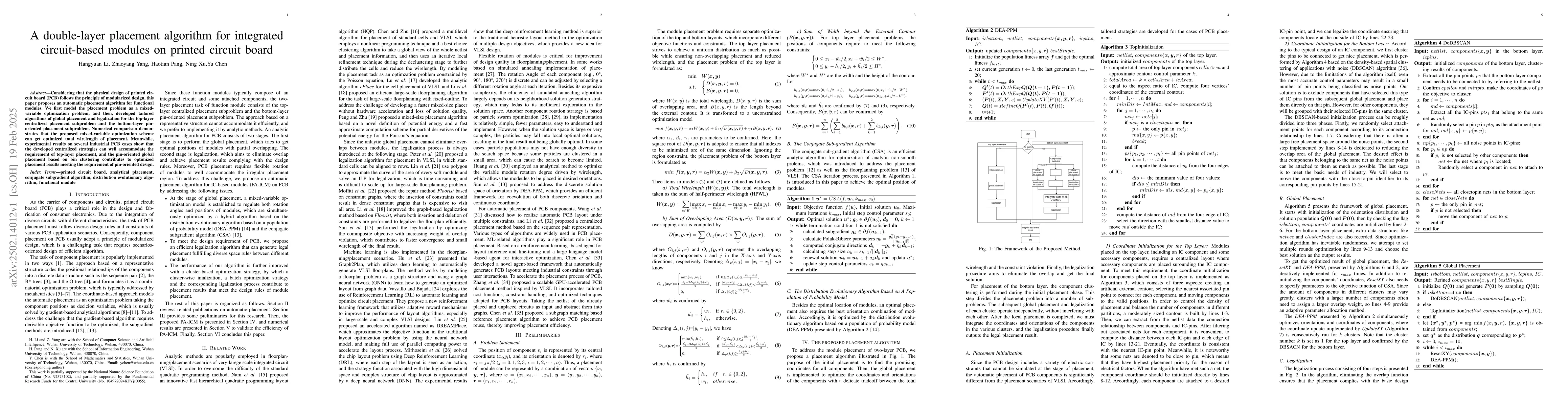
Considering that the physical design of printed circuit board (PCB) follows the principle of modularized design, this paper proposes an automatic placement algorithm for functional modules. We first model the placement problem as a mixed-variable optimization problem, and then, developed tailored algorithms of global placement and legalization for the top-layer centralized placement subproblem and the bottom-layer pin-oriented placement subproblem. Numerical comparison demonstrates that the proposed mixed-variable optimization scheme can get optimized total wirelength of placement. Meanwhile, experimental results on several industrial PCB cases show that the developed centralized strategies can well accommodate the requirement of top-layer placement, and the pin-oriented global placement based on bin clustering contributes to optimized placement results meeting the requirement of pin-oriented design.

AI Key Findings

Generated Jun 11, 2025

Methodology

The paper proposes a double-layer placement algorithm for integrated circuit-based modules on printed circuit boards, formulating the problem as a mixed-variable optimization problem and developing tailored algorithms for global placement and legalization for top and bottom layers.

Key Results

  • The proposed mixed-variable optimization scheme achieves optimized total wirelength of placement.
  • Experimental results on industrial PCB cases demonstrate that centralized strategies well accommodate top-layer placement requirements.
  • Pin-oriented global placement based on bin clustering contributes to optimized placement results meeting pin-oriented design requirements.
  • Numerical comparison shows the algorithm outperforms metaheuristics-based algorithms on representative structure codes.
  • The algorithm successfully addresses both top-layer and bottom-layer placement issues in industrial PCB cases.

Significance

This research is significant as it presents an efficient automatic placement algorithm for PCB design, which can handle modularized design principles and optimize wirelength, thereby improving the performance and manufacturability of PCBs.

Technical Contribution

The paper introduces a double-layer placement algorithm with tailored global optimization and legalization strategies for top and bottom layer placements, utilizing a mixed-variable optimization model.

Novelty

The novelty of this work lies in its mixed-variable optimization approach for PCB placement, addressing both top and bottom layers with tailored strategies, and its successful validation on industrial PCB cases.

Limitations

  • The algorithm's performance might degrade when dealing with cases where bottom IC-pinpoint density is very concentrated.
  • The density-based clustering algorithm may cluster IC-pinpoints into a concentrated distribution, increasing the challenge of global placement.
  • Splitting multiple netlists by clusters might affect the overall connectivity between pinpoints of some nets.

Future Work

  • Improve performance on large-scale cases.
  • Incorporate the module placement method to automate the design of PCBs consisting of several functional modules.

Paper Details

PDF Preview

Download PDF

Key Terms

No key terms available for this paper.

Citation Network

Current paper (gray), citations (green), references (blue)

Current Paper
Citations
References
Click to view

No citations found for this paper.

Comments (0)

This website uses cookies to ensure you get the best experience. Learn more