Summary
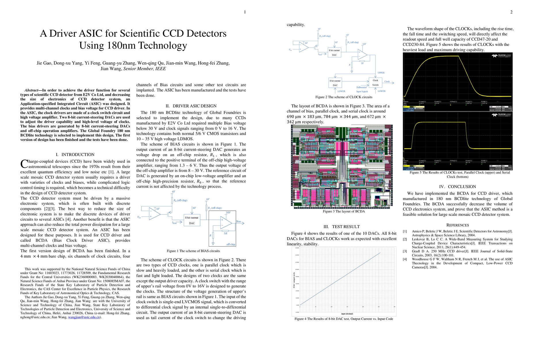
In order to achieve the driver function for several types of scientific CCD detector from E2V Co Ltd, and decreasing the size of electronics of CCD detector system, an Application-specified Integrated Circuit (ASIC) was designed. It provides multi-channel clocks and bias voltage for CCD driver. In the ASIC, the clock drivers are made of a clock switch circuit and high voltage amplifier. Two 8-bit current-steering DACs are used to adjust the driver capability and high-level voltage of clocks. The bias drivers are generated by 8-bit current-steering DACs and off-chip operation amplifiers. The Global Foundry 180 nm BCDlite technology is selected to implement this design. The first version of design has been finished and the tests have been done.
AI Key Findings
Get AI-generated insights about this paper's methodology, results, and significance.
Paper Details
PDF Preview
Key Terms
Citation Network
Current paper (gray), citations (green), references (blue)
Display is limited for performance on very large graphs.
Similar Papers
Found 4 papersNo citations found for this paper.

Comments (0)