Publication
Metrics
AI Quick Summary
This paper provides a detailed guide for fabricating planar silicon quantum dot heterostructures, emphasizing the importance of material properties and fabrication processes to avoid defects and disorder. The guide also outlines the use of tailored oxidation, vapor deposition, and atomic-layer deposition techniques to create electrostatically defined quantum dots.
Paper Preview
Abstract
We describe important considerations to create top-down fabricated planar quantum dots in silicon, often not discussed in detail in literature. The subtle interplay between intrinsic material properties, interfaces and fabrication processes plays a crucial role in the formation of electrostatically defined quantum dots. Processes such as oxidation, physical vapor deposition and atomic-layer deposition must be tailored in order to prevent unwanted side effects such as defects, disorder and dewetting. In two directly related manuscripts written in parallel we use techniques described in this work to create depletion-mode quantum dots in intrinsic silicon, and low-disorder silicon quantum dots defined with palladium gates. While we discuss three different planar gate structures, the general principles also apply to 0D and 1D systems, such as self-assembled islands and nanowires.
AI Key Findings
Get AI-generated insights about this paper's methodology, results, significance, and more — seven facets brought into focus.
Impact
Paper Details
PDF Preview
Key Terms
Citation Network
Current paper (gray), citations (green), references (blue)
Display is limited for performance on very large graphs.
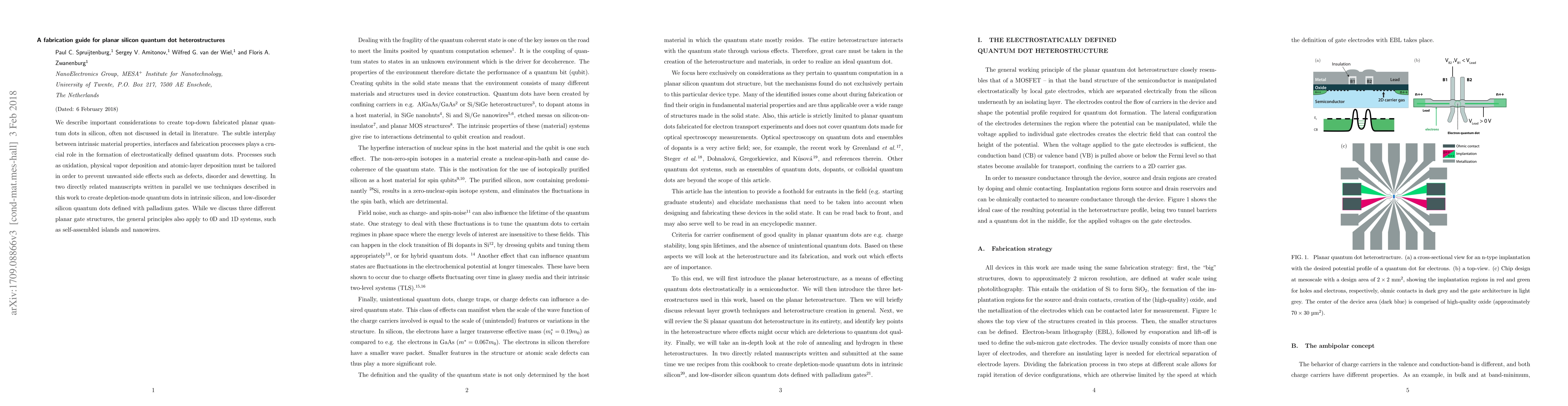
Discussion 0