Publication
Metrics
AI Quick Summary
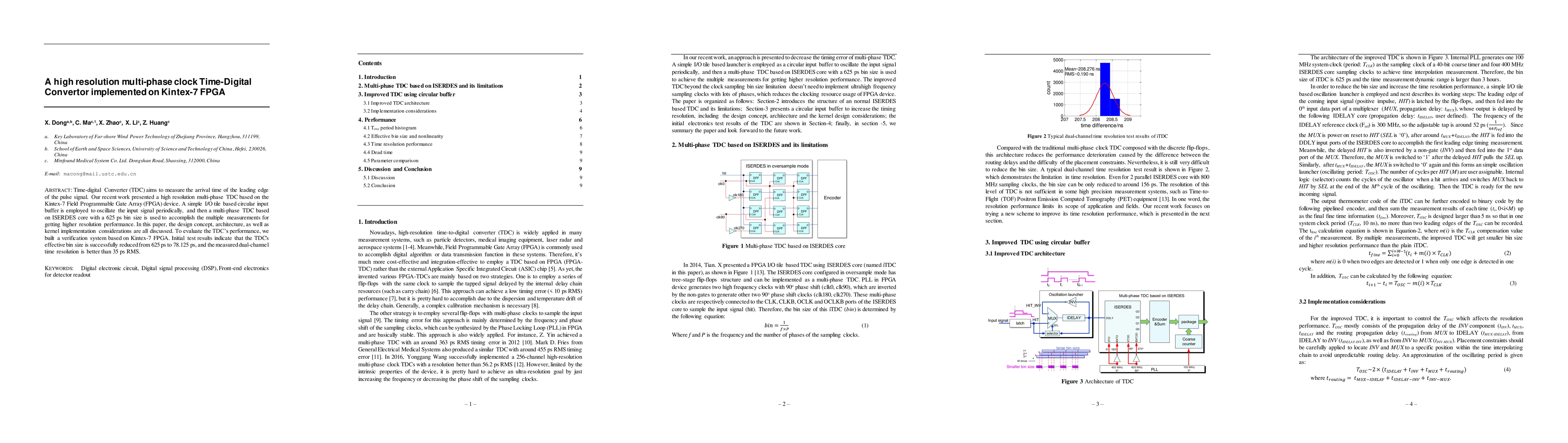
This paper presents a high-resolution multi-phase Time-Digital Converter (TDC) implemented on a Kintex-7 FPGA, achieving a bin size reduction from 625 ps to 78.125 ps and a dual-channel time resolution better than 35 ps RMS. The design utilizes an ISERDES core and a circular input buffer for improved measurement accuracy.
Paper Preview
Abstract
Time-digital Converter (TDC) aims to measure the arrival time of the leading edge of the pulse signal. Our recent work presented a high resolution multi-phase TDC based on the Kintex-7 Field Programmable Gate Array (FPGA) device. A simple I/O tile based circular input buffer is employed to oscillate the input signal periodically, and then a multi-phase TDC based on ISERDES core with a 625 ps bin size is used to accomplish the multiple measurements for getting higher resolution performance. In this paper, the design concept, architecture, as well as kernel implementation considerations are all discussed. To evaluate the TDC's performance, we built a verification system based on Kintex-7 FPGA. Initial test results indicate that the TDC's effective bin size is successfully reduced from 625 ps to 78.125 ps, and the measured dual-channel time resolution is better than 35 ps RMS.
AI Key Findings
Get AI-generated insights about this paper's methodology, results, significance, and more — seven facets brought into focus.
Impact
Paper Details
Authors
PDF Preview
Key Terms
Citation Network
Current paper (gray), citations (green), references (blue)
Display is limited for performance on very large graphs.
Discussion 0