Publication
Metrics
AI Quick Summary
This paper describes an atomtronic transistor circuit functioning as a driven matterwave oscillator, revealing two oscillation threshold regimes linked to Bose-Einstein condensation and negative transresistance. The oscillation thresholds depend on potential energy differences, and the circuit's operation is observed via in-trap and time-of-flight absorption imaging.
Paper Preview
Abstract
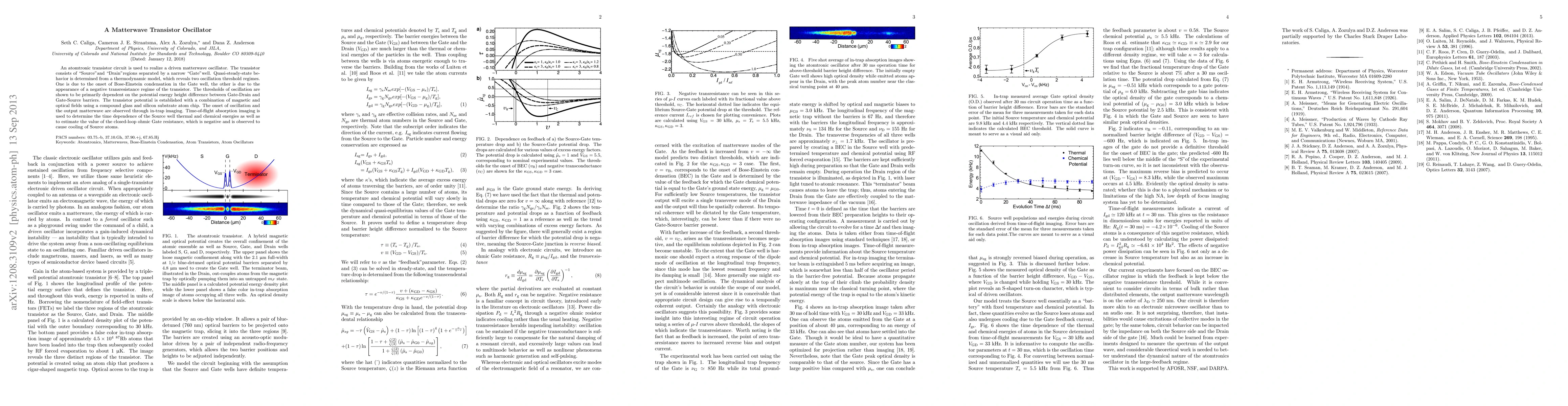
An atomtronic transistor circuit is used to realize a driven matterwave oscillator. The transistor consists of Source and Drain regions separated by a narrow Gate well. Quasi-steady-state behavior is determined from a thermodynamic model, which reveals two oscillation threshold regimes. One is due to the onset of Bose-Einstein condensation in the Gate well, the other is due to the appearance of a negative transresistance regime of the transistor. The thresholds of oscillation are shown to be primarily dependent on the potential energy height difference between Gate-Drain and Gate-Source barriers. The transistor potential is established with a combination of magnetic and optical fields using a compound glass and silicon substrate atom chip. The onset of oscillation and the output matterwave are observed through in-trap imaging. Time-of-flight absorption imaging is used to determine the time dependence of the Source well thermal and chemical energies as well as to estimate the value of the closed-loop ohmic Gate resistance, which is negative and is observed to cause cooling of Source atoms.
AI Key Findings
Get AI-generated insights about this paper's methodology, results, significance, and more — seven facets brought into focus.
Impact
Paper Details
PDF Preview
Key Terms
Citation Network
Current paper (gray), citations (green), references (blue)
Display is limited for performance on very large graphs.
Discussion 0