A Packaging Method for ALPIDE Integration Enabling Flexible and Low-Material-Budget Designs

Source: ArXiv

AI Quick Summary

This research introduces a novel flexible packaging method for ALPIDE chips using thin aluminum and polyimide cables bonded via single-point Tape Automated Bonding (spTAB), replacing traditional wire bonding for non-planar designs. The proposed solution maintains an ultra-low material budget and is demonstrated through a prototype at Fondazione Bruno Kessler and INFN TIFPA laboratories.

Share: Share on X LinkedIn

Summary

This work presents a novel solution for the packaging of ALPIDE chips that facilitates non-planar assembly with a minimal material budget. This solution represents a technological advancement based on methodologies developed for the ALICE ITS1 and the STAR tracker two decades ago. The core of this approach involves the use of flexible cables composed of aluminum and polyimide, with thicknesses on the order of tens of micrometers. These cables are connected to the sensors using single-point Tape Automated Bonding (spTAB), which replaces the traditional wire bonding technique that is suboptimal for curved integrations. The spTAB bonding is achieved by creating openings in the polyimide layer, allowing aluminum wires to remain free-standing, which are then connected to the sensor using pressure and ultrasonic energy. Extending this concept, we have applied this approach to entire printed circuit boards (PCBs), resulting in a fully flexible packaging solution maintaining an ultra-low material budget. This work introduces a prototype utilizing this method to bond an ALPIDE chip, proposing it as a viable option for future designs necessitating flexible packaging for both the chip and associated electronics. The overall workflow, comprising microfabrication and assembly, is carried out at the Fondazione Bruno Kessler and INFN TIFPA laboratories and will be detailed to elucidate our procedures and demonstrate the applicability of our solution in future experimental setups. The proposed packaging features 
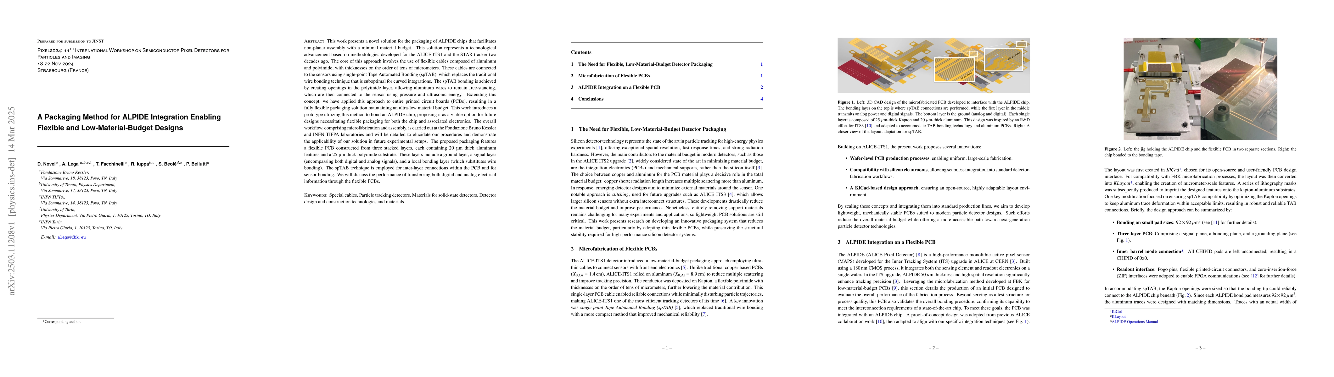
a flexible PCB constructed from three stacked layers, each containing 20 $\mu$m thick aluminum features and a 25 $\mu$m thick polyimide substrate. These layers include a ground layer, a signal layer (encompassing both digital and analog signals), and a local bonding layer (which substitutes wire bonding).

AI Key Findings

Generated Jun 10, 2025

Methodology

The research presents a novel packaging method for ALPIDE chips using flexible cables composed of aluminum and polyimide, connected via single-point Tape Automated Bonding (spTAB). This approach replaces traditional wire bonding, enabling non-planar assembly with minimal material budget.

Key Results

  • Development of a flexible packaging solution for ALPIDE chips using ultra-thin, flexible PCBs.
  • Successful integration of an ALPIDE chip onto a flexible PCB using spTAB bonding.
  • Demonstration of the method's applicability to entire PCBs, maintaining an ultra-low material budget.

Significance

This research is important as it addresses the need for lightweight, mechanically stable PCBs in modern particle detector designs, reducing overall material budget while offering a more accessible path to next-generation particle detection technologies.

Technical Contribution

The main technical contribution is the development of a flexible packaging method for ALPIDE chips using thin, aluminum-polyimide cables and spTAB bonding, which replaces traditional wire bonding and enables non-planar assembly.

Novelty

This work builds upon earlier methodologies from ALICE ITS1 and STAR tracker, introducing wafer-level PCB production, compatibility with silicon cleanrooms, and a Kicad-based design approach for open-source, adaptable layouts.

Limitations

  • The current work focuses on proof-of-concept and further optimization is needed for signal transmission through flexible PCBs.
  • Impedance mismatches and their impact on signal integrity require further investigation and refinement of the design.

Future Work

  • Detailed signal integrity analysis, such as eye-diagram testing, to assess the flexible PCB's effect on signal quality.
  • Thermal and mechanical stress testing to ensure reliable performance in operational environments.

Paper Details

PDF Preview

Download PDF

Citation Network

Current paper (gray), citations (green), references (blue)

Display is limited for performance on very large graphs.

Current Paper
Citations
References
Click to view

No citations found for this paper.

Comments (0)

This website uses cookies to ensure you get the best experience. Learn more