Publication
Metrics
AI Quick Summary
This paper presents a silicon nanocrystal Field Effect Transistor (ncFET) that operates similarly to a Tunnelling Field Effect Transistor (TFET), featuring two barriers in series fabricated in thin silicon dioxide and intrinsic polycrystalline silicon, achieving a 10$^4$ on/off current ratio and low leakage current without doping challenges.
Paper Preview
Abstract
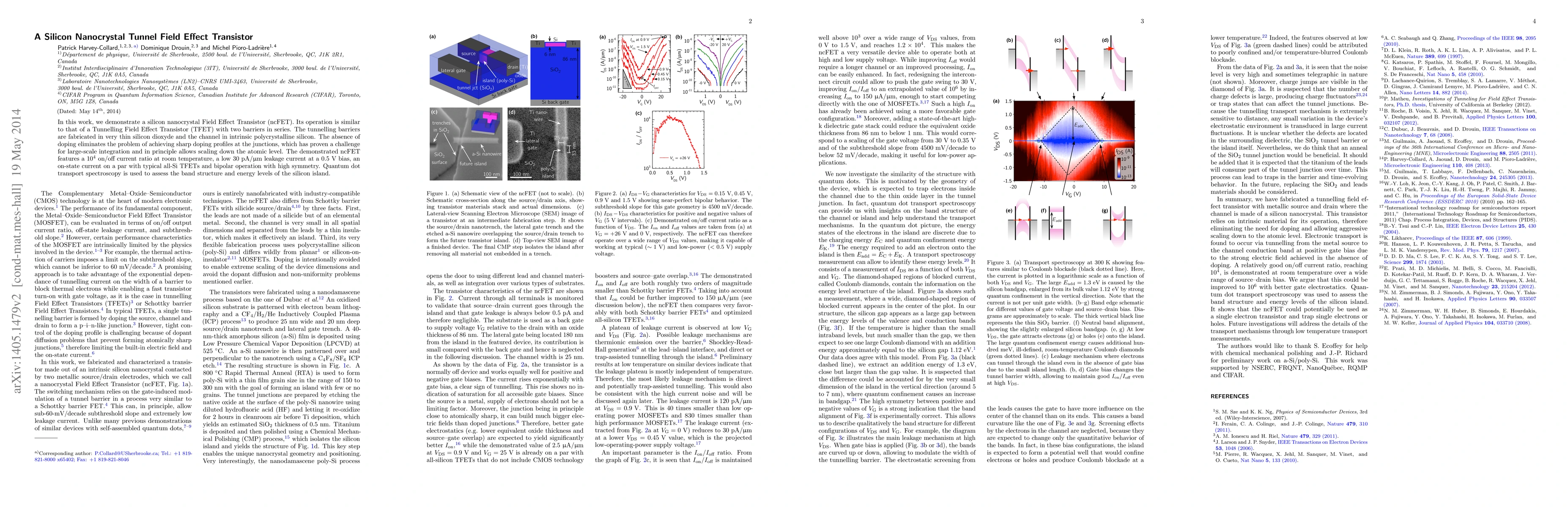
In this work, we demonstrate a silicon nanocrystal Field Effect Transistor (ncFET). Its operation is similar to that of a Tunnelling Field Effect Transistor (TFET) with two barriers in series. The tunnelling barriers are fabricated in very thin silicon dioxyde and the channel in intrinsic polycrystalline silicon. The absence of doping eliminates the problem of achieving sharp doping profiles at the junctions, which has proven a challenge for large-scale integration and in principle allows scaling down the atomic level. The demonstrated ncFET features a 10$^4$ on/off current ratio at room temperature, a low 30 pA/$\mu$m leakage current at a 0.5 V bias, an on-state current on a par with typical all-Si TFETs and bipolar operation with high symmetry. Quantum dot transport spectroscopy is used to assess the band structure and energy levels of the silicon island.
AI Key Findings
Get AI-generated insights about this paper's methodology, results, significance, and more — seven facets brought into focus.
Impact
Paper Details
PDF Preview
Key Terms
Citation Network
Current paper (gray), citations (green), references (blue)
Display is limited for performance on very large graphs.
Discussion 0