Summary
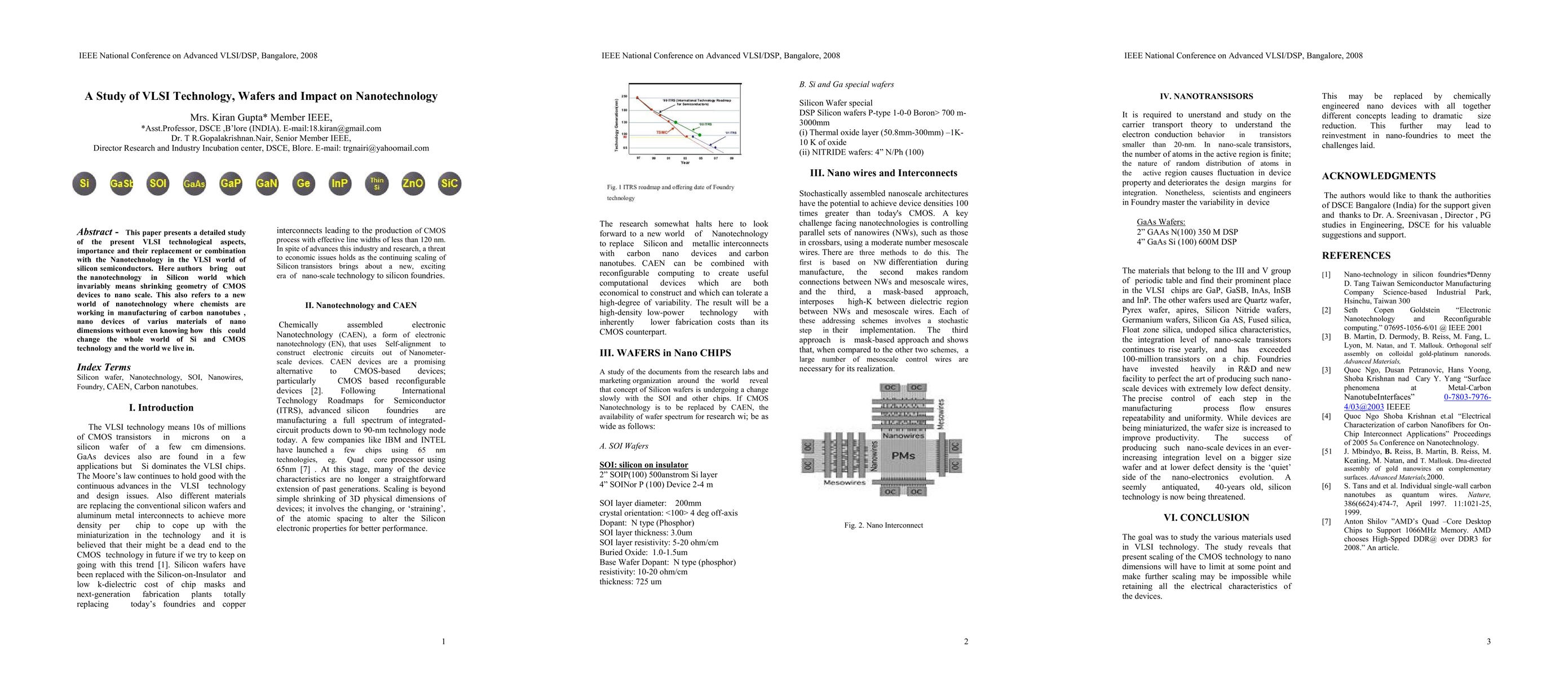
This paper presents a detailed study of the present VLSI technological aspects, importance and their replacement or combination with the Nanotechnology in the VLSI world of silicon semiconductors. Here authors bring out the nanotechnology in Silicon world which invariably means shrinking geometry of CMOS devices to nano scale. This also refers to a new world of nanotechnology where chemists are working in manufacturing of carbon nanotubes , nano devices of varius materials of nano dimensions without even knowing how this could change the whole world of Si and CMOS technology and the world we live in.
AI Key Findings
Get AI-generated insights about this paper's methodology, results, and significance.
Paper Details
PDF Preview
Key Terms
Citation Network
Current paper (gray), citations (green), references (blue)
Display is limited for performance on very large graphs.
Similar Papers
Found 4 papersAI/ML Algorithms and Applications in VLSI Design and Technology
Zia Abbas, Andleeb Zahra, Deepthi Amuru et al.
| Title | Authors | Year | Actions |
|---|
Comments (0)