Publication
Metrics
AI Quick Summary
This paper presents a compact, home-built system capable of performing both deterministic transfer processes for freestanding semiconductors and 2D materials, and contact photolithography for micro-scale pattern fabrication, achieving feature sizes of ~1-2 um. The system shares a precision translation stage and optical microscope for both functions.
Paper Preview
Abstract
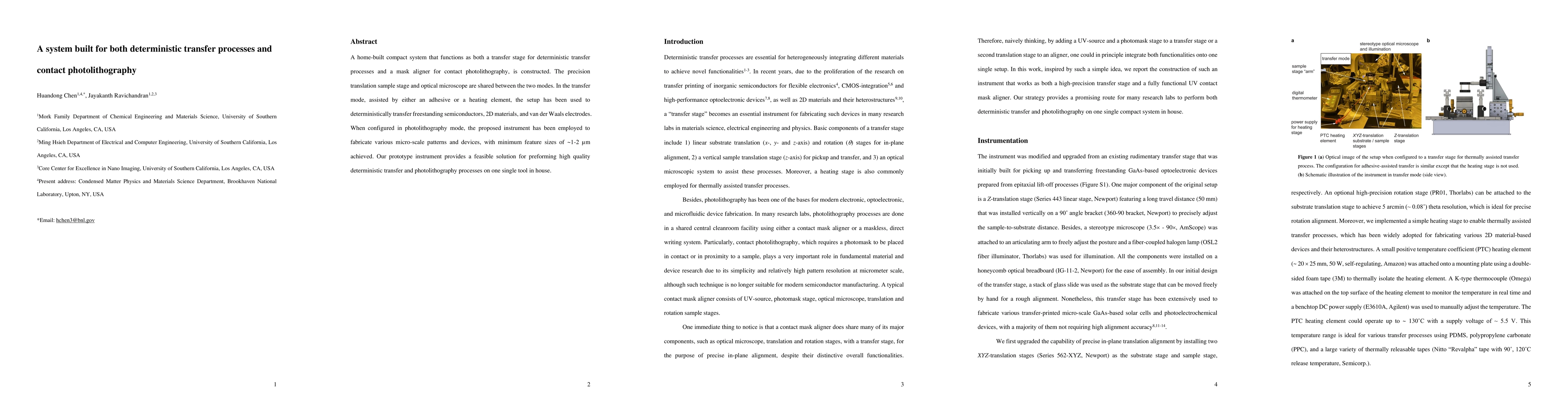
A home-built compact system that functions as both a transfer stage for deterministic transfer processes and a mask aligner for contact photolithography, is constructed. The precision translation sample stage and optical microscope are shared between the two modes. In the transfer mode, assisted by either an adhesive or a heating element, the setup has been used to deterministically transfer freestanding semiconductors, 2D materials, and van der Waals electrodes. When configured in photolithography mode, the proposed instrument has been employed to fabricate various micro-scale patterns and devices, with minimum feature sizes of ~1-2 um achieved. Our prototype instrument provides a feasible solution for preforming high quality deterministic transfer and photolithography processes on one single tool in house.
AI Key Findings
Get AI-generated insights about this paper's methodology, results, significance, and more — seven facets brought into focus.
Impact
Paper Details
Authors
PDF Preview
Key Terms
Citation Network
Current paper (gray), citations (green), references (blue)
Display is limited for performance on very large graphs.
Discussion 0