Summary
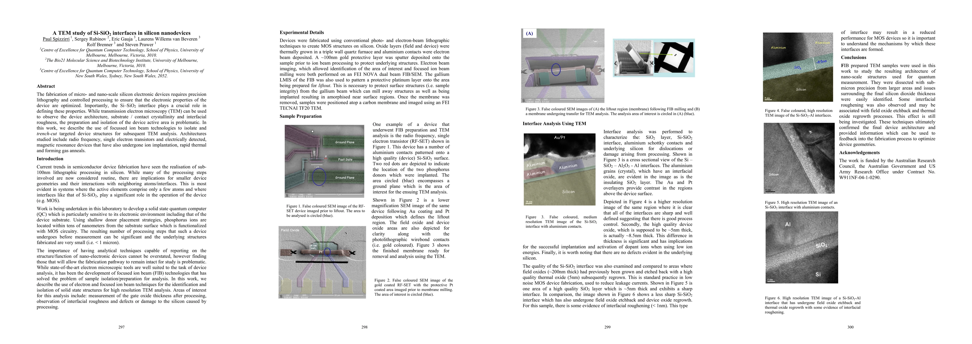
The fabrication of micro- and nano-scale silicon electronic devices requires precision lithography and controlled processing to ensure that the electronic properties of the device are optimized. Importantly, the Si-SiO2 interface plays a crucial role in defining these properties. While transmission electron microscopy (TEM) can be used to observe the device architecture, substrate / contact crystallinity and interfacial roughness, the preparation and isolation of the device active area is problematic. In this work, we describe the use of focussed ion beam technologies to isolate and trench-cut targeted device structures for subsequent TEM analysis. Architectures studied include radio frequency, single electron transistors and electrically detected, magnetic resonance devices that have also undergone ion implantation, rapid thermal and forming gas anneals.
AI Key Findings
Get AI-generated insights about this paper's methodology, results, and significance.
Paper Details
PDF Preview
Key Terms
Similar Papers
Found 4 papers| Title | Authors | Year | Actions |
|---|

Comments (0)