ArxivLens

Quick Summary:

Summary: This research introduces a cost-effective two-step wet-etching method for fabricating nanopores in silicon. The method involves a double-sided initial etching followed by track-etching, and utilizes a custom fixture for effective processing, along with an electrochemical system for monitoring ion diffusion, achieving successful nanopore fabrication.

Journal Reference: Dans Symposium on Design, Test, Integration and Packaging of MEMS/MOEMS - DTIP 2007, Stresa, lago Maggiore : Italie (2007)
arXiv Id: 0802.3087
Comments: Submitted on behalf of EDA Publishing Association (http://irevues.inist.fr/EDA-Publishing)
Date Published: 2008-02-22
Date Updated: 2008-02-22

Categories:

Key Terms (TF-IDF):

silicon (0.352)
track (0.284)
effectively (0.282)
proposed method (0.233)
pre (0.216)
cost (0.210)
record (0.192)
sided (0.188)
cavities (0.188)
method (0.166)
results indicate (0.160)
hold (0.159)
carried (0.152)
ion (0.148)
inside (0.147)
employed (0.144)
proposed (0.144)
detect (0.141)
diffusion (0.136)
double (0.133)

Summary:

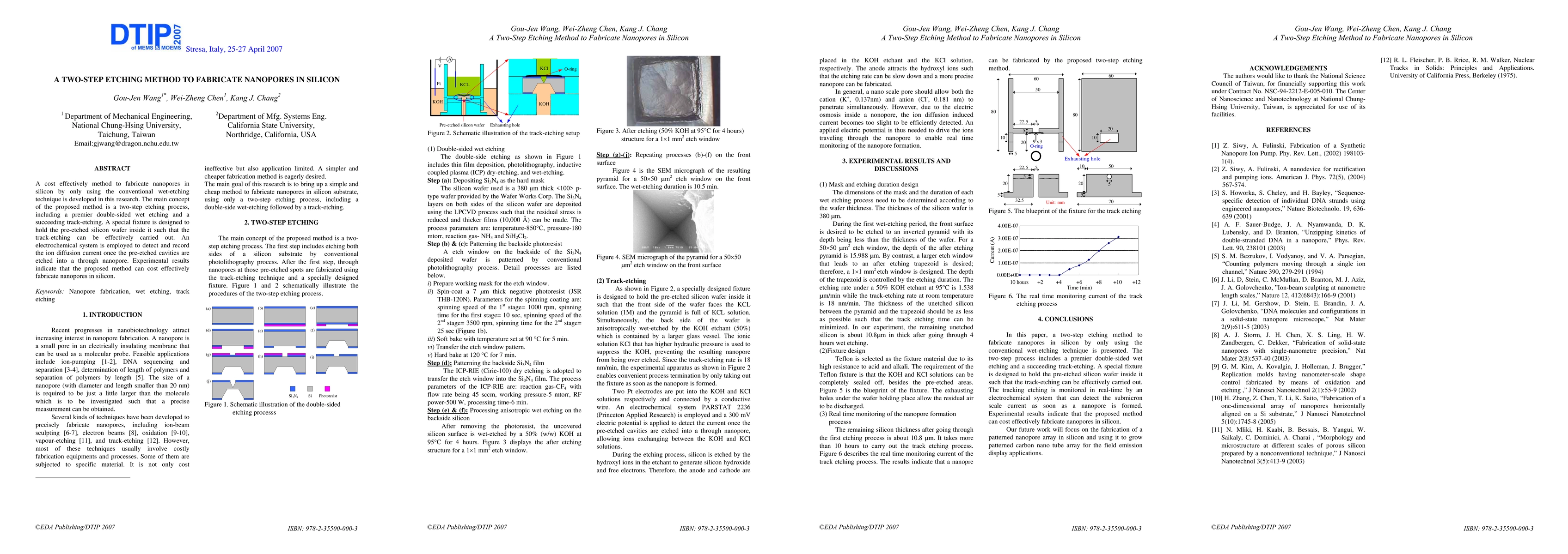
A cost effectively method to fabricate nanopores in silicon by only using the conventional wet-etching technique is developed in this research. The main concept of the proposed method is a two-step etching process, including a premier double-sided wet etching and a succeeding track-etching. A special fixture is designed to hold the pre-etched silicon wafer inside it such that the track-etching can be effectively carried out. An electrochemical system is employed to detect and record the ion diffusion current once the pre-etched cavities are etched into a through nanopore. Experimental results indicate that the proposed method can cost effectively fabricate nanopores in silicon.

Citation & Reference Network Visualization

This graph shows how this paper is connected to other research. The current paper is shown in dark gray, papers that cite it are in green, and papers it references are in blue. You can:

Current Paper
Papers citing this work (Citations)
Papers cited by this work (References)

• Hover over any node to see the paper title

• Click a node to view that paper's details

• Drag nodes to rearrange the graph

• Use the zoom controls (bottom right) to zoom in/out

Citations and References

Title Authors Year Actions
A Metal-Solution FET Enhanced Proton-Motive-Force Driving Photovoltaic
Gou-Jen Wang, Ming‐Way Lee, Wei-Zheng Chen, Yi-Hong Chen, Ming-Chun Chien, Mingming Yu
2011
View Paper
Fabrication and electrical characterization of a pore–cavity–pore device
D. Pedone, Martin Langecker, A. M. Münzer, Ruoshan Wei, Robin D. Nagel, U. Rant
2010
View Paper
Electrophoretic deposition of uniformly distributed TiO2 nanoparticles using an anodic aluminum oxide template for efficient photolysis
Gou-Jen Wang, S.W. Chou
2010
View Paper
Nanopore Size Estimation by Electrochemical Impedance Spectroscopy Analysis
Ming-Chun Chien, Gou-Jen Wang, Ming Yu
2008
View Paper
FABRICATION OF SWNTs FOR WATER DESALINATION AND MULTILAYER STRUCTURE FOR DNA SEQUENCING
Jingyuan Yao
2012
View Paper

Similar Papers

Ultra-Thin, High-Lifetime Silicon Nitride Membranes for Nanopore Sensing

Shankar Dutt, Y. M. Nuwan D. Y. Bandara, Patrick Kluth, Buddini I. Karawdeniya, Nahid Afrin

Published: 2023-03-30

Thermophysical Characteristics of the Porous Silicon Samples Formed by Electrochemical, Chemical and Combined Etching Methods

A. Serikkanov, B. Zhumabay, R. Dagarbek, D. Kantarbayeva, I. Nevmerzhitsky, B. Rakymetov, Zh. Alsar, K. B. Tynyshtykbayev, Z. Insepov

Published: 2023-08-22

Fabrication of a Silicon Electron Multiplier sensor using Metal Assisted Chemical Etching and its characterisation

Victor Coco, Heidi Sandaker, Marius Mæhlum Halvorsen, Paula Collins, Lucia Romano

Published: 2024-01-25

Comments (0)

This website uses cookies to ensure you get the best experience. Learn more