A VLSI Design Flow for Secure Side-Channel Attack Resistant ICs
Publication
Metrics
AI Quick Summary
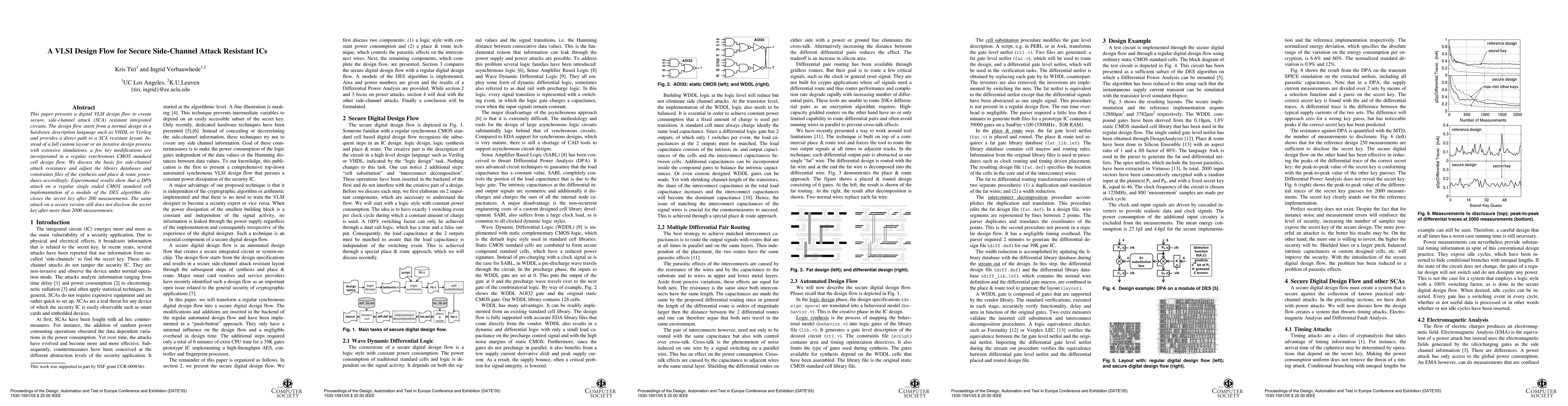
This paper introduces a streamlined VLSI design flow for creating secure, side-channel attack resistant integrated circuits by modifying standard CMOS design processes. Experimental results demonstrate significant resistance to differential power analysis attacks, with the secure version resisting key disclosure after 2000 measurements compared to 200 for a regular implementation.
Paper Preview
Abstract
This paper presents a digital VLSI design flow to create secure, side-channel attack (SCA) resistant integrated circuits. The design flow starts from a normal design in a hardware description language such as VHDL or Verilog and provides a direct path to a SCA resistant layout. Instead of a full custom layout or an iterative design process with extensive simulations, a few key modifications are incorporated in a regular synchronous CMOS standard cell design flow. We discuss the basis for side-channel attack resistance and adjust the library databases and constraints files of the synthesis and place & route procedures accordingly. Experimental results show that a DPA attack on a regular single ended CMOS standard cell implementation of a module of the DES algorithm discloses the secret key after 200 measurements. The same attack on a secure version still does not disclose the secret key after more than 2000 measurements.
AI Key Findings
Get AI-generated insights about this paper's methodology, results, significance, and more — seven facets brought into focus.
Impact
Paper Details
PDF Preview
Key Terms
Citation Network
Current paper (gray), citations (green), references (blue)
Display is limited for performance on very large graphs.
Discussion 0