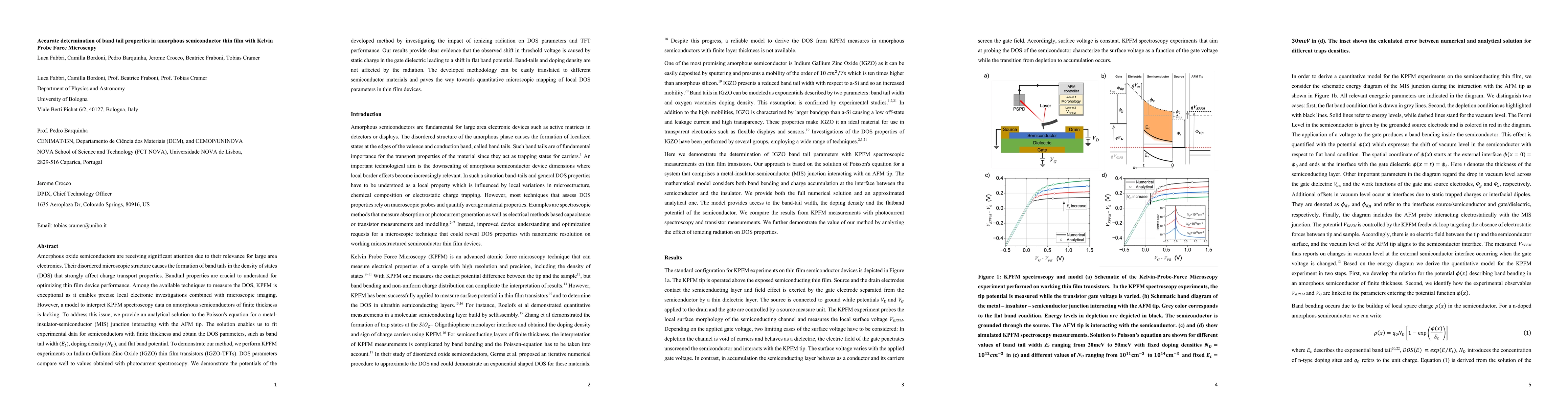
Summary
Amorphous oxide semiconductors are receiving significant attention due to their relevance for large area electronics. Their disordered microscopic structure causes the formation of band tails in the density of states (DOS) that strongly affect charge transport properties. Bandtail properties are crucial to understand for optimizing thin film device performance. Among the available techniques to measure the DOS, KPFM is exceptional as it enables precise local electronic investigations combined with microscopic imaging. However, a model to interpret KPFM spectroscopy data on amorphous semiconductors of finite thickness is lacking. To address this issue, we provide an analytical solution to the Poisson's equation for a metal-insulator-semiconductor (MIS) junction interacting with the AFM tip. The solution enables us to fit experimental data for semiconductors with finite thickness and obtain the DOS parameters, such as band tail width (E_t), doping density (N_D), and flat band potential. To demonstrate our method, we perform KPFM experiments on Indium-Gallium-Zinc Oxide (IGZO) thin film transistors (IGZO-TFTs). DOS parameters compare well to values obtained with photocurrent spectroscopy. We demonstrate the potentials of the developed method by investigating the impact of ionizing radiation on DOS parameters and TFT performance. Our results provide clear evidence that the observed shift in threshold voltage is caused by static charge in the gate dielectric leading to a shift in flat band potential. Band-tails and doping density are not affected by the radiation. The developed methodology can be easily translated to different semiconductor materials and paves the way towards quantitative microscopic mapping of local DOS parameters in thin film devices.
AI Key Findings
Get AI-generated insights about this paper's methodology, results, and significance.
Paper Details
PDF Preview
Key Terms
Citation Network
Current paper (gray), citations (green), references (blue)
Display is limited for performance on very large graphs.
Similar Papers
Found 4 papers| Title | Authors | Year | Actions |
|---|
Comments (0)