Achieving low contact resistance through copper-intercalated bilayer MoS$_2$
Publication
Metrics
AI Quick Summary
This research proposes a method to reduce contact resistance in MoS$_2$-based transistors by intercalating copper between bilayer MoS$_2$, achieving contact resistances close to the quantum limit. The design enables ohmic contacts and lower operating voltages, potentially enhancing the performance of 2D electronic devices.
Paper Preview
Abstract
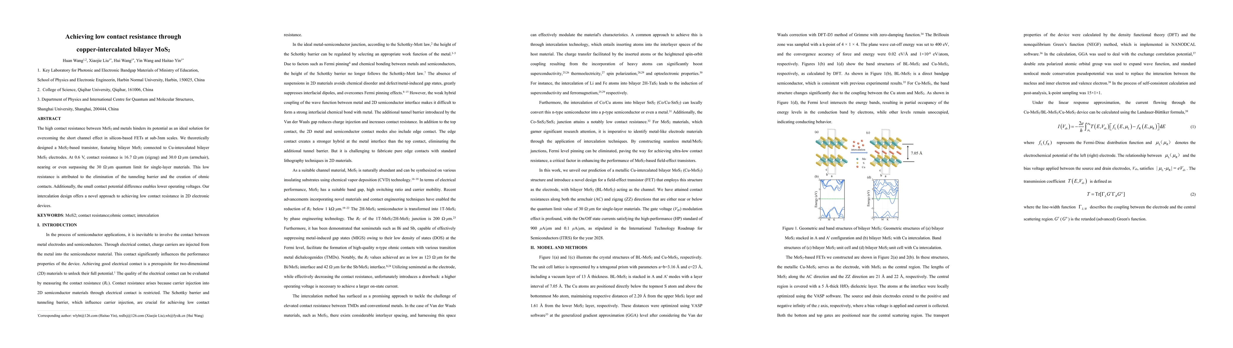
The high contact resistance between MoS$_2$ and metals hinders its potential as an ideal solution for overcoming the short channel effect in silicon-based FETs at sub-3nm scales. We theoretically designed a MoS$_2$-based transistor, featuring bilayer MoS$_2$ connected to Cu-intercalated bilayer MoS$_2$ electrodes. At 0.6 V, contact resistance is 16.7 $\Omega \cdot \mu$m (zigzag) and 30.0 $\Omega \cdot \mu$m (armchair), nearing or even surpassing the 30 $\Omega \cdot \mu$m quantum limit for single-layer materials. This low resistance is attributed to the elimination of the tunneling barrier and the creation of ohmic contacts. Additionally, the small contact potential difference enables lower operating voltages. Our intercalation design offers a novel approach to achieving low contact resistance in 2D electronic devices.
AI Key Findings
Get AI-generated insights about this paper's methodology, results, significance, and more — seven facets brought into focus.
Paper Details
Authors
PDF Preview
Related Papers
No references found for this paper.
Discussion 0