Advanced In-Design Auto-Fixing Flow for Cell Abutment Pattern Matching Weakpoints
Publication
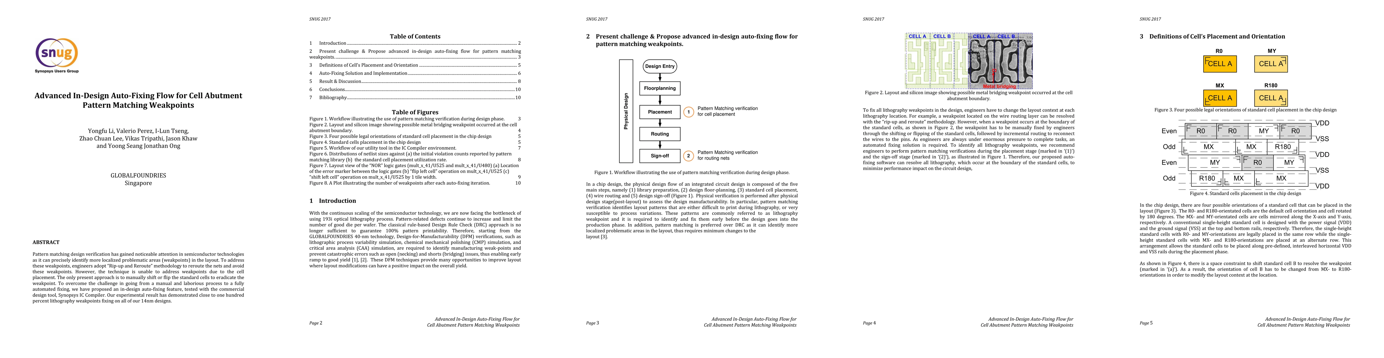
Metrics
AI Quick Summary
Researchers developed an in-design auto-fixing feature to address weakpoints in semiconductor designs, achieving over 90% success rate on 14nm designs.
Paper Preview
Abstract
Pattern matching design verification has gained noticeable attention in semiconductor technologies as it can precisely identify more localized problematic areas (weakpoints) in the layout. To address these weakpoints, engineers adopt 'Rip-up and Reroute' methodology to reroute the nets and avoid these weakpoints. However, the technique is unable to address weakpoints due to the cell placement. The only present approach is to manually shift or flip the standard cells to eradicate the weakpoint. To overcome the challenge in going from a manual and laborious process to a fully automated fixing, we have proposed an in-design auto-fixing feature, tested with the commercial design tool, Synopsys IC Compiler. Our experimental result has demonstrated close to one hundred percent lithography weakpoints fixing on all of our 14nm designs.
AI Key Findings
Get AI-generated insights about this paper's methodology, results, significance, and more — seven facets brought into focus.
Impact
Paper Details
PDF Preview
Key Terms
Citation Network
Current paper (gray), citations (green), references (blue)
Display is limited for performance on very large graphs.
Discussion 0