Publication
Metrics
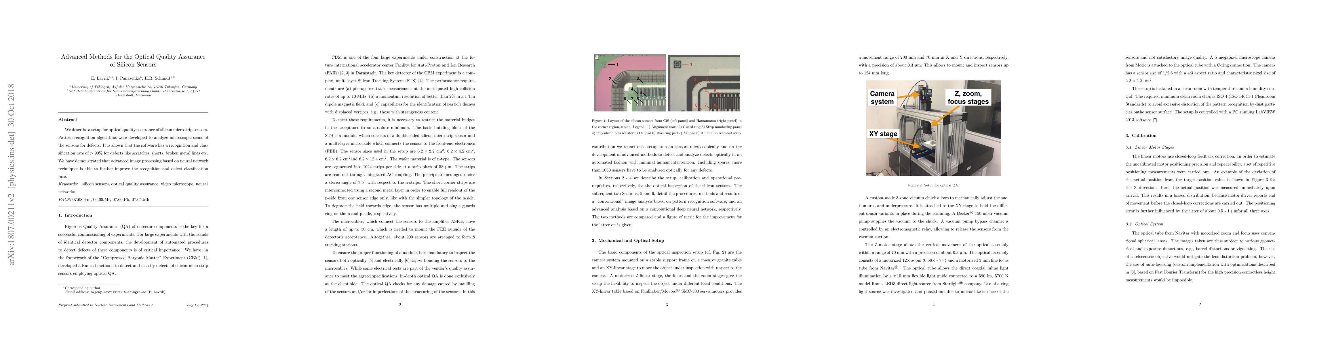
AI Quick Summary
Researchers developed an optical quality assurance setup for silicon microstrip sensors using pattern recognition algorithms with a high accuracy rate of >90% for detecting defects such as scratches and broken metal lines. Neural network-based image processing further improved the defect classification rate.
Paper Preview
Abstract
We describe a setup for optical quality assurance of silicon microstrip sensors. Pattern recognition algorithms were developed to analyze microscopic scans of the sensors for defects. It is shown that the software has a recognition and classification rate of $>$~90\% for defects like scratches, shorts, broken metal lines etc. We have demonstrated that advanced image processing based on neural network techniques is able to further improve the recognition and defect classification rate.
AI Key Findings
Get AI-generated insights about this paper's methodology, results, significance, and more — seven facets brought into focus.
Impact
Paper Details
PDF Preview
Key Terms
Citation Network
Current paper (gray), citations (green), references (blue)
Display is limited for performance on very large graphs.
Discussion 0