Advanced scanning probe lithography
Publication
Metrics
Paper Preview
Abstract
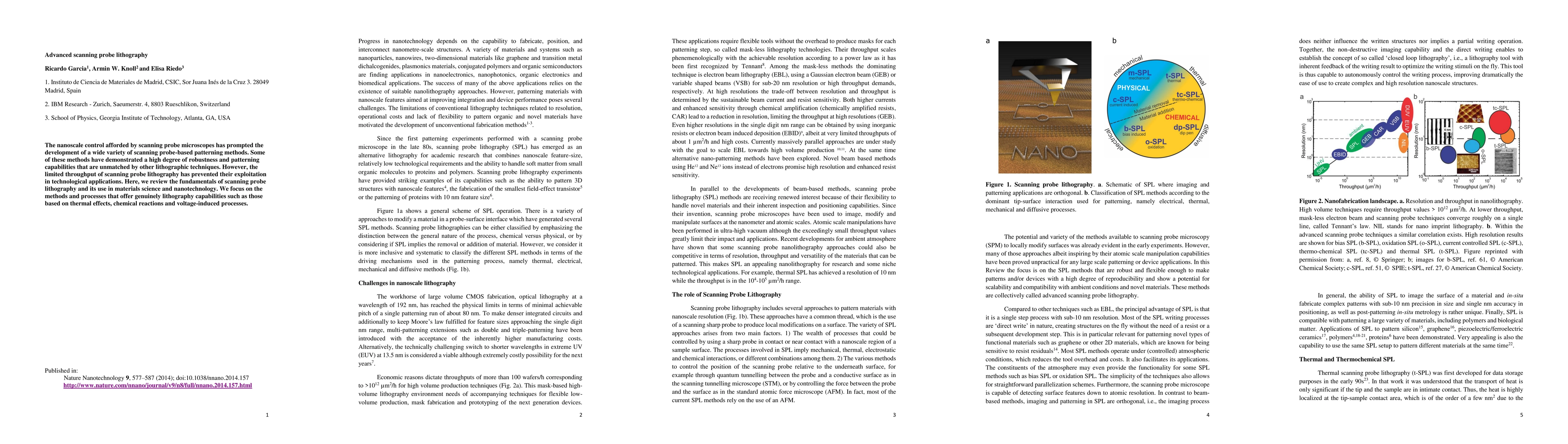
The nanoscale control afforded by scanning probe microscopes has prompted the development of a wide variety of scanning probe-based patterning methods. Some of these methods have demonstrated a high degree of robustness and patterning capabilities that are unmatched by other lithographic techniques. However, the limited throughput of scanning probe lithography has prevented their exploitation in technological applications. Here, we review the fundamentals of scanning probe lithography and its use in materials science and nanotechnology. We focus on the methods and processes that offer genuinely lithography capabilities such as those based on thermal effects, chemical reactions and voltage-induced processes.
AI Key Findings — Failed
Key findings generation failed. Failed to start generation process
Impact
Paper Details
PDF Preview
Key Terms
Citation Network
Current paper (gray), citations (green), references (blue)
Display is limited for performance on very large graphs.
Discussion 0