The paper provides a comprehensive review of entangled photon pair generation in 2D van der Waals materials, discussing fundamental principles, optical quantum characterization techniques, and key physical parameters associated with quantum states.
Advancements in Entangled Photon Pairs in 2D Van der Waals Materials for On-chip Quantum Applications
Publication
Metrics
AI Quick Summary
This review highlights advancements in generating entangled photon pairs using 2D van der Waals materials, crucial for quantum technologies. It discusses generation principles, characterization techniques, and potential for on-chip integration, while outlining current limitations and future prospects.
Quick Answers
What is "Advancements in Entangled Photon Pairs in 2D Van der Waals Materials for On-chip Quantum Applications" about?
This review highlights advancements in generating entangled photon pairs using 2D van der Waals materials, crucial for quantum technologies. It discusses generation principles, characterization techniques, and potential for on-chip integration, while outlining current limitations and future prospects.
What methodology did the authors use?
The paper provides a comprehensive review of entangled photon pair generation in 2D van der Waals materials, discussing fundamental principles, optical quantum characterization techniques, and key physical parameters associated with quantum states. More in Methodology →
What are the key results?
Recent breakthroughs in entangled photon pair generation in 2D vdW materials are highlighted. — Various optical quantum characterization techniques for these materials are reviewed. More in Key Results →
Why is this work significant?
This research is crucial for advancing quantum technologies, including high-precision sensors, communication, computing, and cryptography, by leveraging scalable on-chip quantum photonic devices based on 2D vdW materials. More in Significance →
What are the main limitations?
The paper outlines current limitations in the field without specifying them in detail. — More experimental data and in-depth analysis could strengthen the findings. More in Limitations →
Abstract
The next generation of technology is rooted in quantum-based advancements. The entangled photon pair sources play a pivotal role in a wide range of advanced quantum applications, including quantum high precision sensors, communication, computing, cryptography and so on. Scalable on-chip quantum photonic devices have the potential to drive game changing developments in this field. This review article highlights recent breakthroughs in the generation of entangled photon pairs in two dimensional (2D) van der Waals (vdW) materials, with a focus on their applicability to quantum technologies and plausible on-chip integration technology. The article begins by discussing the fundamental principles of entangled photon pairs generation. It provides a comprehensive review of the origin and generation of entangled photons in emerging vdW materials, alongside various optical quantum characterization techniques. The review then explores key physical parameters of the quantum states associated with entangled photon pairs. Additionally, it examines concepts related to the realization of paired photon generation at the quantum limit. The final section focuses on the potential for on-chip integrated quantum device applications. Beyond highlighting recent advancements in quantum-based research, the review also outlines current limitations and future prospects aimed at advancing the field
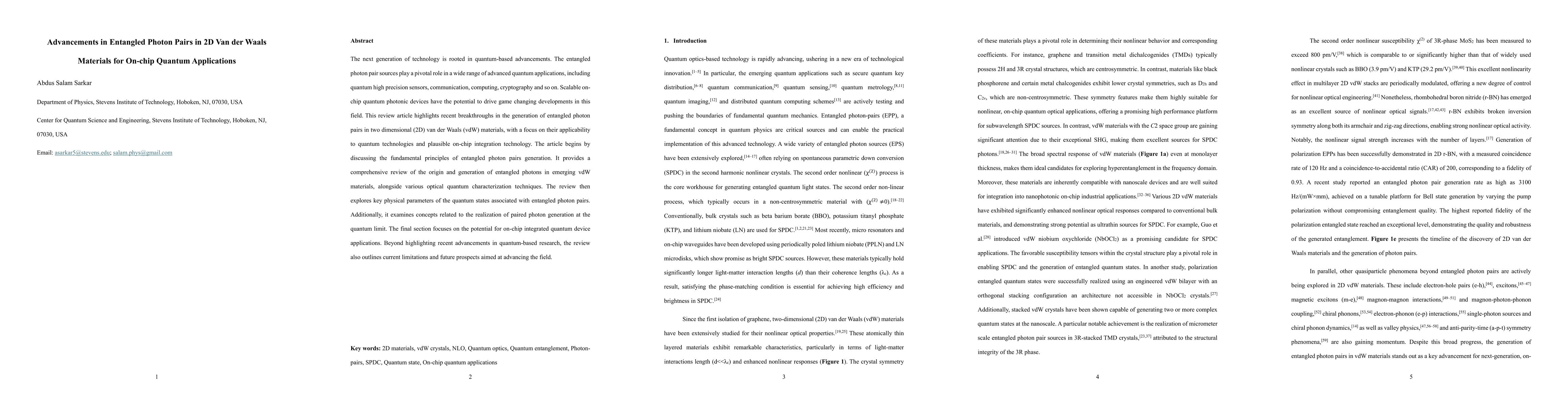
Key Findings, in focus
Seven facets of this paper, analysed and brought into focus by AI.
This research is crucial for advancing quantum technologies, including high-precision sensors, communication, computing, and cryptography, by leveraging scalable on-chip quantum photonic devices based on 2D vdW materials.
- Recent breakthroughs in entangled photon pair generation in 2D vdW materials are highlighted.
- Various optical quantum characterization techniques for these materials are reviewed.
- Physical parameters of quantum states linked to entangled photon pairs are explored.
- Concepts for realizing paired photon generation at the quantum limit are examined.
- Potential for on-chip integrated quantum device applications is discussed.
This research is crucial for advancing quantum technologies, including high-precision sensors, communication, computing, and cryptography, by leveraging scalable on-chip quantum photonic devices based on 2D vdW materials.
The paper contributes by reviewing and summarizing the current state of entangled photon pair generation in 2D van der Waals materials, emphasizing their potential for on-chip quantum applications.
This work stands out by focusing on 2D van der Waals materials, which are emerging platforms for entangled photon pair generation, and by stressing their applicability to on-chip quantum technologies.
- The paper outlines current limitations in the field without specifying them in detail.
- More experimental data and in-depth analysis could strengthen the findings.
- Exploration of new 2D vdW materials for entangled photon pair generation.
- Development of improved on-chip integration technologies for quantum devices.
Paper Details
Authors
PDF Preview
Related Papers
No references found for this paper.
Discussion 0