Summary
We introduce scanning-probe-assisted nanowire circuitry (SPANC) as a new method to fabricate electrodes for the characterization of electrical transport properties at the nanoscale. SPANC uses an atomic force microscope (AFM) to manipulate nanowires to create complex and highly conductive nanostructures (paths) that work as nanoelectrodes, allowing connectivity and electrical characterization of other nano-objects. The paths are formed by the spontaneous cold welding of gold nanowires upon mechanical contact, leading to an excellent contact resistance of about 9 Ohms/junction. SPANC is an easy to use and cost-effective technique that fabricates clean nanodevices. Hence, this new method can complement and/or be an alternative to other well-established methods to fabricate nanocircuits such as electron beam lithography (EBL). The circuits made by SPANC are easily reconfigurable, and their fabrication does not require the use of polymers and chemicals. In this work, we present a few examples that illustrate the capabilities of this method, allowing robust device fabrication and electrical characterization of several nano-objects with sizes down to aprox. 10 nm, well below the current smallest size able to be contacted in a device using the standard available technology (around 30 nm). Importantly, we also provide the first experimental determination of the sheet resistance of thin antimonene flakes.
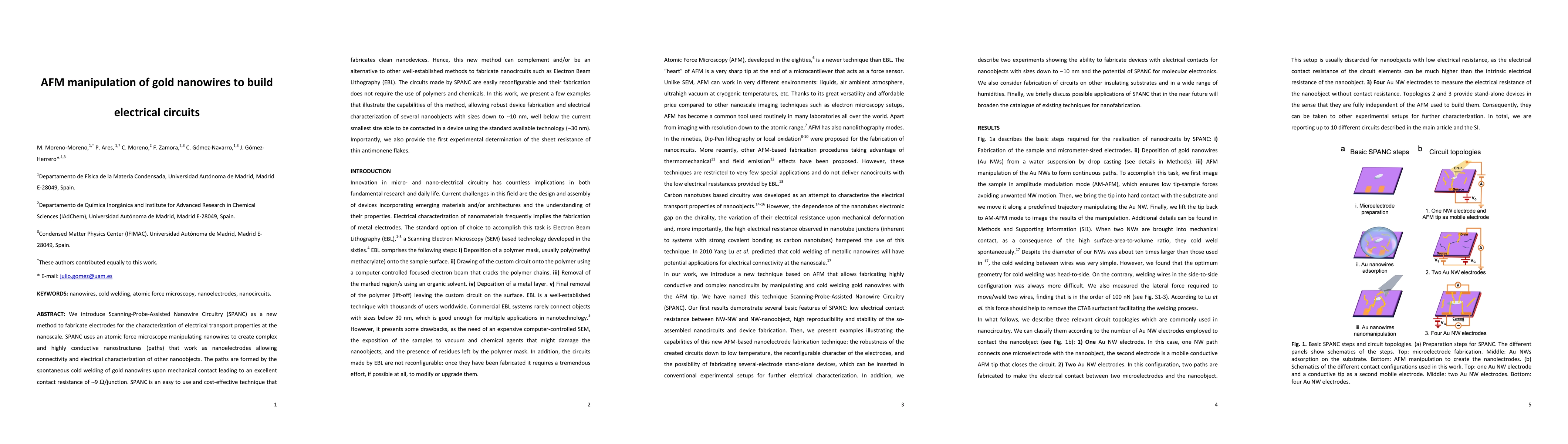
AI Key Findings
Get AI-generated insights about this paper's methodology, results, and significance.
Paper Details
PDF Preview
Key Terms
Citation Network
Current paper (gray), citations (green), references (blue)
Display is limited for performance on very large graphs.
Similar Papers
Found 4 papers| Title | Authors | Year | Actions |
|---|
Comments (0)