Publication
Metrics
AI Quick Summary
This paper introduces and evaluates All-Back-Schottky-Contact (ABSC) thin-film photovoltaic devices using 2D simulations, demonstrating that the design minimizes charge transport interfaces and eliminates the need for front contacts and pn junctions. Optimal efficiency near 20% is achieved through careful passivation of front surfaces and back contacts.
Paper Preview
Abstract
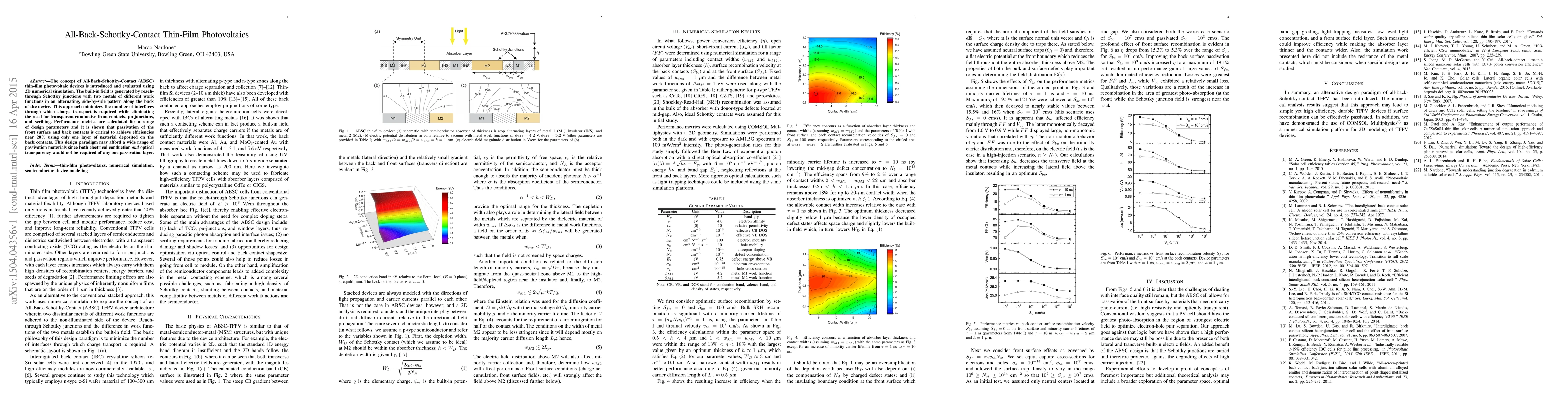
The concept of All-Back-Schottky-Contact (ABSC) thin-film photovoltaic devices is introduced and evaluated using 2D numerical simulation. The built-in field is generated by reach-through Schottky junctions with two metals of different work functions in an alternating, side-by-side pattern along the back of the device. This approach minimizes the number of interfaces through which charge transport is required while eliminating the need for transparent conductive front contacts, pn junctions, and scribing. Performance metrics are calculated for a range of design parameters and it is shown that passivation of the front surface and back contacts is critical to achieve efficiencies near 20% using only one layer of material deposited on the back contacts. This design paradigm may afford a wide range of passivation materials since both electrical conduction and optical transparency would not be required of any one passivation layer.
AI Key Findings
Get AI-generated insights about this paper's methodology, results, significance, and more — seven facets brought into focus.
Impact
Paper Details
PDF Preview
Key Terms
Citation Network
Current paper (gray), citations (green), references (blue)
Display is limited for performance on very large graphs.
Discussion 0