All-dielectric metasurface for wavefront control at terahertz frequencies
Publication
Metrics
AI Quick Summary
This paper presents a silicon metasurface composed of sub-wavelength silicon cross resonators that converts Gaussian beams into vortex beams at terahertz frequencies. The metasurface achieves high transmittance and phase coverage from 0 to $2\pi$ by tuning the dimensions of the silicon cross resonators, enabling wavefront control and potential applications in molecular fingerprinting and secondary molecular structure detection.
Paper Preview
Abstract
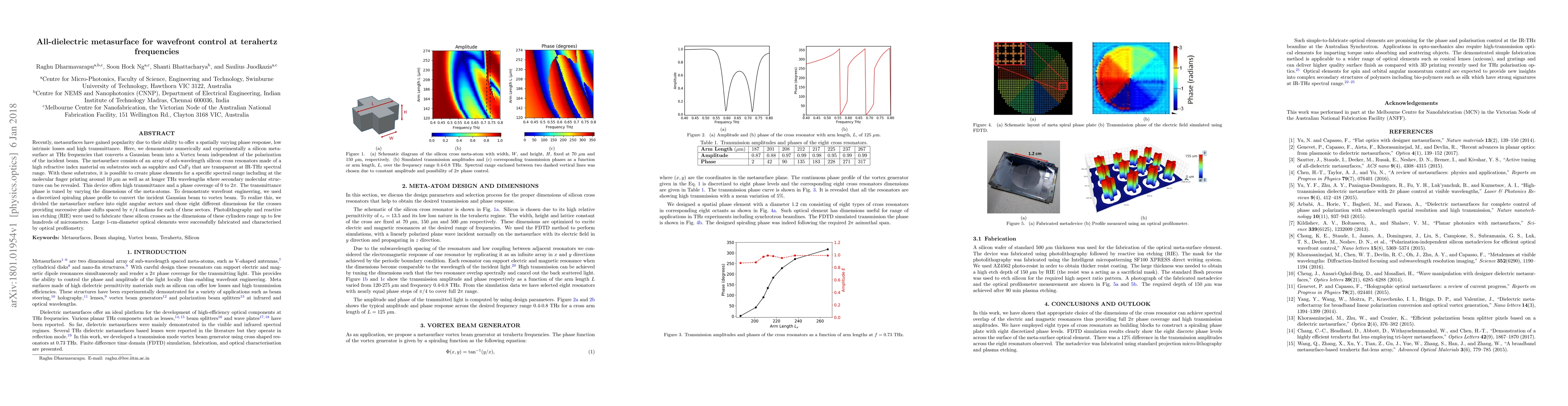
Recently, metasurfaces have gained popularity due to their ability to offer a spatially varying phase response, low intrinsic losses and high transmittance. Here, we demonstrate numerically and experimentally a silicon metasurface at THz frequencies that converts a Gaussian beam into a Vortex beam independent of the polarization of the incident beam. The metasurface consists of an array of sub-wavelength silicon cross resonators made of a high refractive index material on substrates such as sapphire and CaF$_2$ that are transparent at IR-THz spectral range. With these substrates, it is possible to create phase elements for a specific spectral range including at the molecular finger printing around 10$~\mu$m as well as at longer THz wavelengths where secondary molecular structures can be revealed. This device offers high transmittance and a phase coverage of 0 to $2\pi$. The transmittance phase is tuned by varying the dimensions of the meta-atoms. To demonstrate wavefront engineering, we used a discretized spiraling phase profile to convert the incident Gaussian beam to vortex beam. To realize this, we divided the metasurface surface into eight angular sectors and chose eight different dimensions for the crosses providing successive phase shifts spaced by $\pi/4$ radians for each of these sectors. Photolithography and reactive ion etching (RIE) were used to fabricate these silicon crosses as the dimensions of these cylinders range up to few hundreds of micrometers. Large 1-cm-diameter optical elements were successfully fabricated and characterised by optical profilometry.
AI Key Findings
Get AI-generated insights about this paper's methodology, results, significance, and more — seven facets brought into focus.
Impact
Paper Details
PDF Preview
Key Terms
Citation Network
Current paper (gray), citations (green), references (blue)
Display is limited for performance on very large graphs.
Discussion 0