01
MethodologyHow they did it
The research employed a standard CMOS process flow to fabricate an SOI Quantum Dot device with two Gates.
This paper demonstrates the electrical control of electron spin in an SOI Quantum Dot using CMOS technology, and shows how Back-Gate control can switch a hybrid electron spin/valley qubit between a charge-sensitive and a protected state.
This paper demonstrates the electrical control of electron spin in an SOI Quantum Dot using CMOS technology, and shows how Back-Gate control can switch a hybrid electron spin/valley qubit between a charge-sensitive and a protected state.
The research employed a standard CMOS process flow to fabricate an SOI Quantum Dot device with two Gates. More in Methodology →
Electrical-field-mediated control of the spin of electrons confined in an SOI QD was successfully demonstrated experimentally. — Back-Gate control enables switching between electrically-addressable, yet charge noise-sensitive configuration and a protected configuration. More in Key Results →
This research alleviates the trade-off between fast manipulation and long coherence time for compact, scalable, and fault-tolerant quantum logic circuits. More in Significance →
The device geometry was limited by the abrupt interface between the NanoWire and the buried oxide. — Surface roughness variability had a significant impact on the valley splitting energy. More in Limitations →
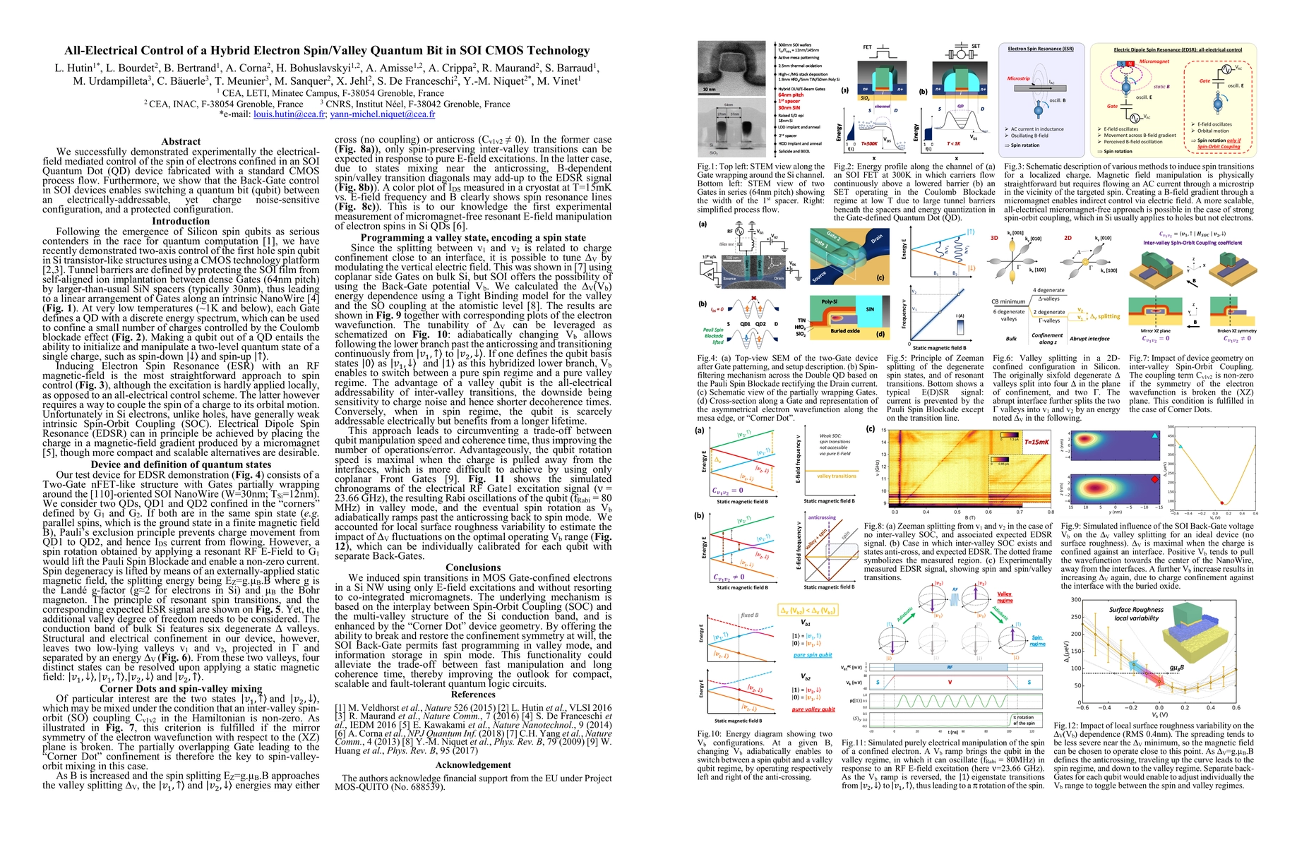
We successfully demonstrated experimentally the electrical-field-mediated control of the spin of electrons confined in an SOI Quantum Dot (QD) device fabricated with a standard CMOS process flow. Furthermore, we show that the Back-Gate control in SOI devices enables switching a quantum bit (qubit) between an electrically-addressable, yet charge noise-sensitive configuration, and a protected configuration.
Seven facets of this paper, analysed and brought into focus by AI.
This research alleviates the trade-off between fast manipulation and long coherence time for compact, scalable, and fault-tolerant quantum logic circuits.
The research employed a standard CMOS process flow to fabricate an SOI Quantum Dot device with two Gates.
This research alleviates the trade-off between fast manipulation and long coherence time for compact, scalable, and fault-tolerant quantum logic circuits.
The SOI Back-Gate voltage Vb enables fast programming in valley mode and information storage in spin mode.
This work demonstrates an all-electrical micromagnet-free approach to induce spin transitions using strong spin-orbit coupling, applicable to electrons.
Current paper (gray), citations (green), references (blue)
Display is limited for performance on very large graphs.
Discussion 0