01
MethodologyHow they did it
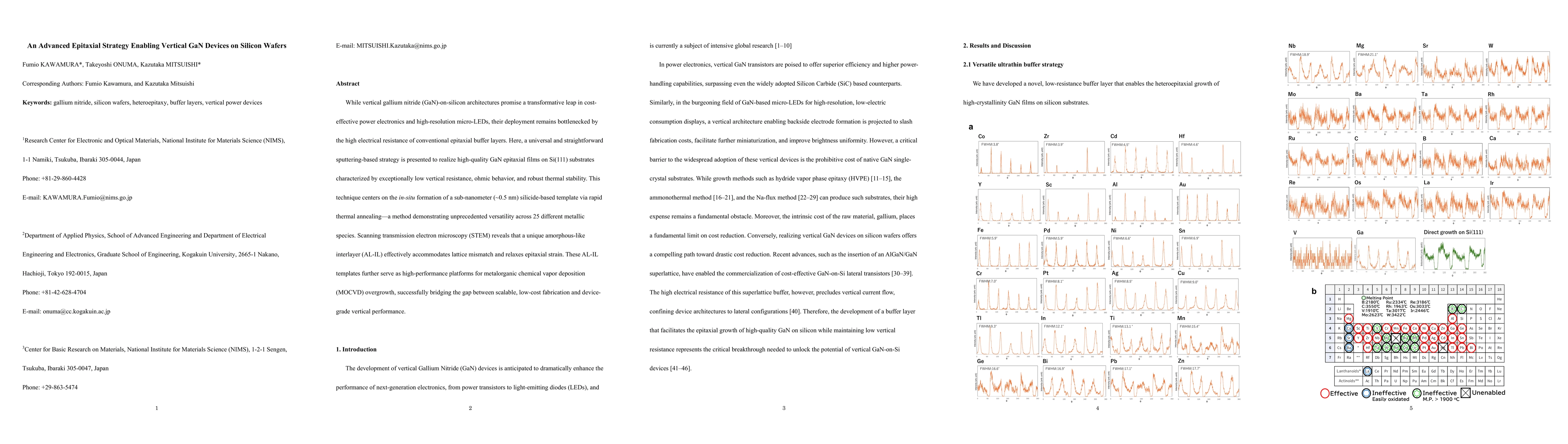
The study proposes a universal sputtering-based strategy to deposit high-quality GaN epitaxial films on Si(111) substrates, followed by in-situ rapid thermal annealing to form a sub-nanometer silicide-based template (~0.5 nm) which creates an amorphous-like interlayer (AL-IL). This AL-IL accommodates lattice mismatch and relaxes epitaxial strain and serves as a platform for subsequent MOCVD overgrowth to achieve device-grade vertical GaN on silicon.
Discussion 0