An all-dielectric bowtie waveguide with deep subwavelength mode confinement
Publication
Metrics
AI Quick Summary
This paper introduces an all-dielectric bowtie (ADB) waveguide that achieves deep subwavelength mode confinement without the high propagation loss typical of plasmonic waveguides, offering a promising solution for future photonic integrated circuits. The ADB waveguide, composed of silicon wedges in a silica cladding, supports a lossless quasi-TM mode, enabling longer propagation lengths and compatibility with semiconductor fabrication.
Paper Preview
Abstract
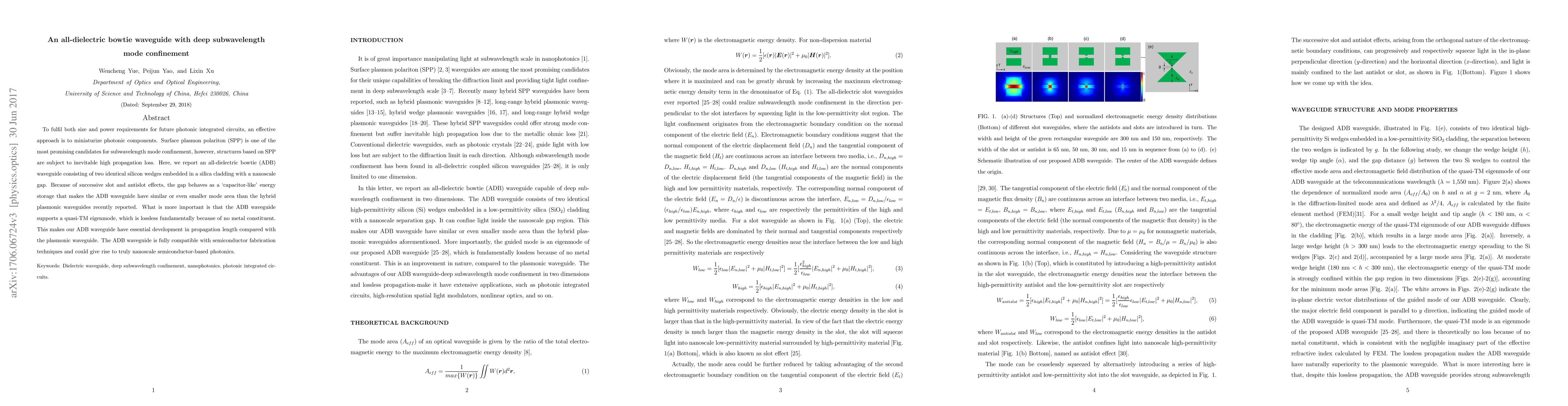
To fulfil both size and power requirements for future photonic integrated circuits, an effective approach is to miniaturize photonic components. Surface plasmon polariton (SPP) is one of the most promising candidates for subwavelength mode confinement, however, structures based on SPP are subject to inevitable high propagation loss. Here, we report an all-dielectric bowtie (ADB) waveguide consisting of two identical silicon wedges embedded in a silica cladding with a nanoscale gap. Because of successive slot and antislot effects, the gap behaves as a 'capacitor-like' energy storage that makes the ADB waveguide have similar or even smaller mode area than the hybrid plasmonic waveguides recently reported. What is more important is that the ADB waveguide supports a quasi-TM eigenmode, which is lossless fundamentally because of no metal constituent. This makes our ADB waveguide have essential development in propagation length compared with the plasmonic waveguide. The ADB waveguide is fully compatible with semiconductor fabrication techniques and could give rise to truly nanoscale semiconductor-based photonics.
AI Key Findings
Get AI-generated insights about this paper's methodology, results, significance, and more — seven facets brought into focus.
Impact
Paper Details
PDF Preview
Key Terms
Citation Network
Current paper (gray), citations (green), references (blue)
Display is limited for performance on very large graphs.
Discussion 0