An Approach to Use Depletion Charges for Modifying Band Profiles for Field-Effect Transistors
Publication
Metrics
AI Quick Summary
This paper investigates using depletion charges from heavily doped regions to modify the band profiles in gate-all-around field-effect transistors (GAAFET), demonstrating significant conduction band profile alterations through simulations. The approach aims to achieve quantum confinement and modify transport properties in an all-Si structure.
Paper Preview
Abstract
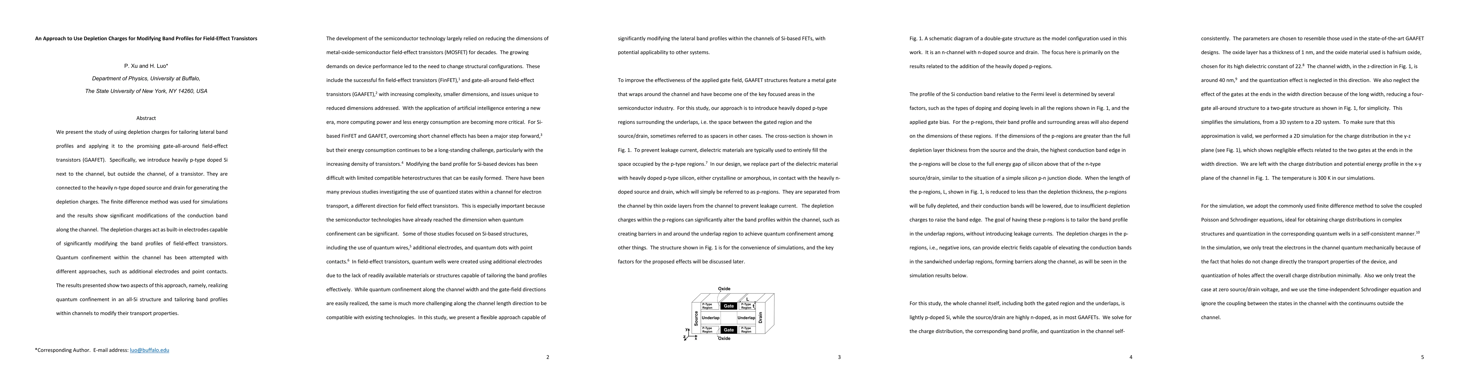
We present the study of using depletion charges for tailoring lateral band profiles and applying it to the promising gate-all-around field-effect transistors (GAAFET). Specifically, we introduce heavily p-type doped Si next to the channel, but outside the channel, of a transistor. They are connected to the heavily n-type doped source and drain for generating the depletion charges. The finite difference method was used for simulations and the results show significant modifications of the conduction band along the channel. The depletion charges act as built-in electrodes capable of significantly modifying the band profiles of field-effect transistors. Quantum confinement within the channel has been attempted with different approaches, such as additional electrodes and point contacts. The results presented show two aspects of this approach, namely, realizing quantum confinement in an all-Si structure and tailoring band profiles within channels to modify their transport properties.
AI Key Findings
Get AI-generated insights about this paper's methodology, results, significance, and more — seven facets brought into focus.
Authors
PDF Preview
Related Papers
No references found for this paper.
Discussion 0