01
MethodologyHow they did it
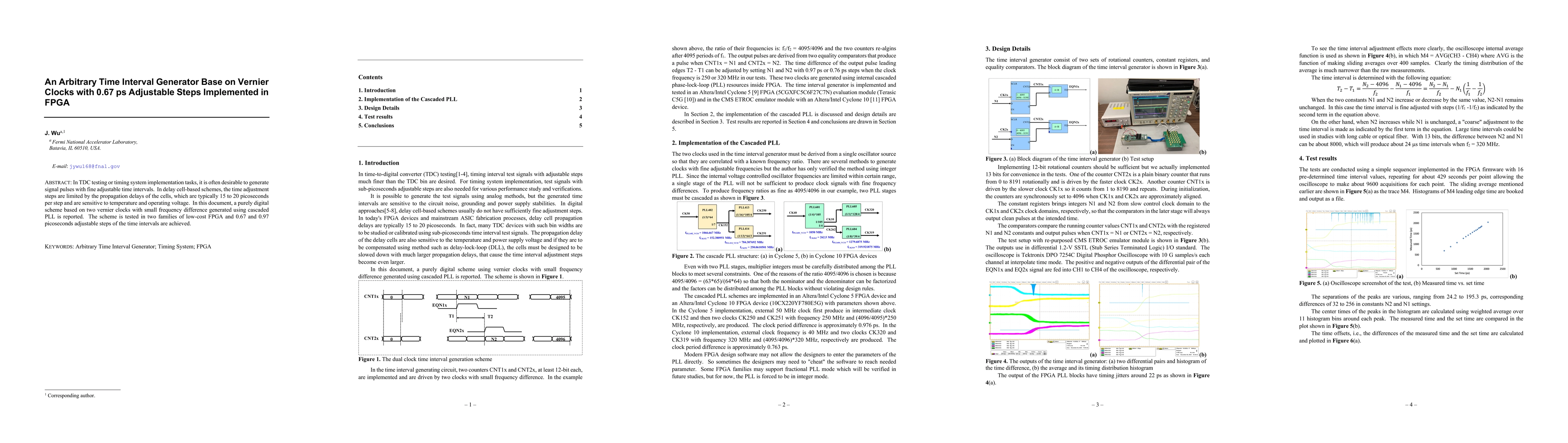
The research implements a purely digital scheme using vernier clocks with small frequency difference generated via cascaded PLL for generating signal pulses with fine adjustable time intervals, tested in two families of low-cost FPGA.
Discussion 0