Publication
Metrics
Quick Actions
AI Quick Summary
Researchers developed an ultra-compact nanophotonic optical modulator that is 10 times smaller than previous silicon modulators, offering improved extinction ratio and operable spectrum.
Quick Answers
What is "An Ultra-compact Nanophotonic Optical Modulator using Multi-State Topological Optimization" about?
Researchers developed an ultra-compact nanophotonic optical modulator that is 10 times smaller than previous silicon modulators, offering improved extinction ratio and operable spectrum.
What methodology did the authors use?
A custom SOI wafer was prepared in-house to deposit a polySi layer, followed by two-step lithography using electron-beam lithography More in Methodology →
What are the key results?
The extinction ratio of the device was measured at λ = 1.55μm and found to be degraded due to fabrication errors — The degradation in extinction ratio was simulated for variation in silicon layer thickness, pixel dimension error, and misalignment between input and output waveguides More in Key Results →
Why is this work significant?
This research demonstrates the importance of precise control over fabrication parameters to achieve high-performance nanophotonic devices More in Significance →
What are the main limitations?
The device fabrication process was limited by the custom SOI wafer preparation and two-step lithography — The results were simulated using numerical models, which may not accurately represent real-world behavior More in Limitations →
Abstract
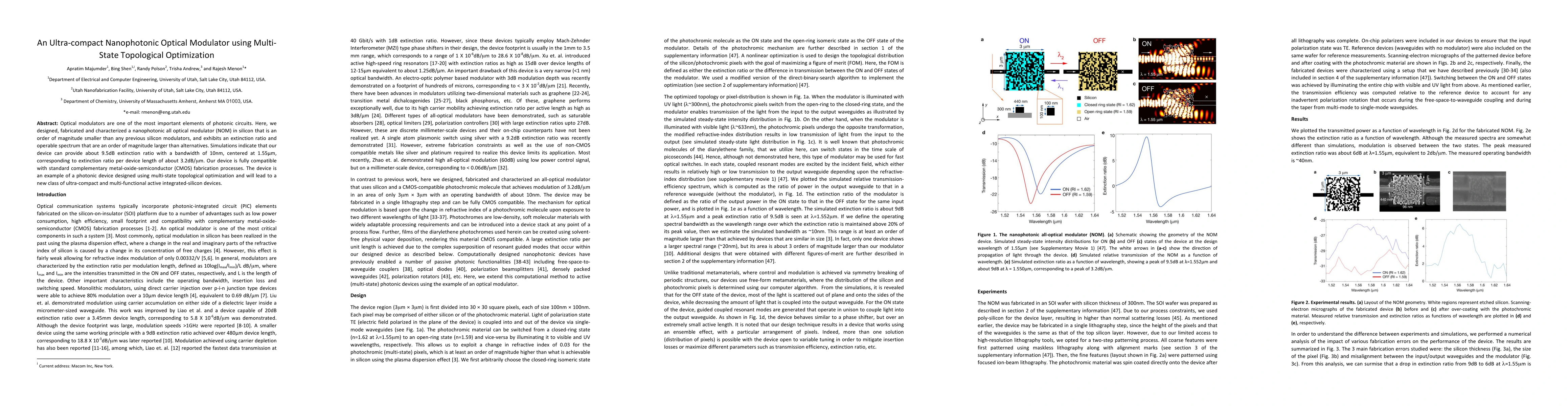
Optical modulators are one of the most important elements of photonic circuits. Here, we designed, fabricated and characterized a nanophotonic all optical modulator (NOM) in silicon that is an order of magnitude smaller than any previous silicon modulators, and exhibits an extinction ratio and operable spectrum that are an order of magnitude larger than alternatives. Simulations indicate that our device can provide about 9.5dB extinction ratio with a bandwidth of 10nm, centered at 1.55um, corresponding to extinction ratio per device length of about 3.2dB/{\mu}m. Our device is fully compatible with standard complementary metal-oxide-semiconductor (CMOS) fabrication processes. The device is an example of a photonic device designed using multi-state topological optimization and will lead to a new class of ultra-compact and multi-functional active integrated-silicon devices.
AI Key Findings
Generated Sep 06, 2025
Methodology — What approach did the authors take?
A custom SOI wafer was prepared in-house to deposit a polySi layer, followed by two-step lithography using electron-beam lithography
Key Results — What are the main findings?
- The extinction ratio of the device was measured at λ = 1.55μm and found to be degraded due to fabrication errors
- The degradation in extinction ratio was simulated for variation in silicon layer thickness, pixel dimension error, and misalignment between input and output waveguides
- The results showed that the main limiting factor is the variation in silicon layer thickness
Significance — Why does this research matter?
This research demonstrates the importance of precise control over fabrication parameters to achieve high-performance nanophotonic devices
Technical Contribution — What is the technical contribution?
A comprehensive simulation model was developed to investigate the effects of fabrication errors on nanophotonic devices
Novelty — What is new about this work?
The use of a custom SOI wafer preparation and two-step lithography in fabricating nanophotonic devices is novel and different from existing research
Limitations — What are the limitations of this study?
- The device fabrication process was limited by the custom SOI wafer preparation and two-step lithography
- The results were simulated using numerical models, which may not accurately represent real-world behavior
Future Work — What did the authors propose for future work?
- Investigating alternative fabrication methods to improve precision and consistency
- Developing more accurate numerical models to simulate device behavior under various conditions
Paper Details
How to Cite This Paper
@article{anon2017an,
title = {An Ultra-compact Nanophotonic Optical Modulator using Multi-State
Topological Optimization},
year = {2017},
eprint = {1712.02835},
archivePrefix = {arXiv},
primaryClass = {physics.app-ph},
}
(2017). An Ultra-compact Nanophotonic Optical Modulator using Multi-State
Topological Optimization. arXiv. https://arxiv.org/abs/1712.02835
"An Ultra-compact Nanophotonic Optical Modulator using Multi-State
Topological Optimization." arXiv, 2017, arxiv.org/abs/1712.02835.
PDF Preview
Key Terms
Citation Network
Current paper (gray), citations (green), references (blue)
Display is limited for performance on very large graphs.
Similar Papers
Found 4 papersInverse-designed nanophotonic neural network accelerators for ultra-compact optical computing
Joel Sved, Shijie Song, Liwei Li et al.
Ultra-compact plexcitonic electro-absorption modulator
Deep Jariwala, Ruoyu Yuan, Jason Lynch
| Title | Authors | Year | Actions |
|---|
Comments (0)