Publication
Metrics
AI Quick Summary
This paper introduces an innovative auto zeroing technique for a three-stage CMOS amplifier, combining high-speed, low power, and minimal input interference, tailored for Ultra-Wide Band flash ADCs. Simulations in ADS validate its operation at 1.2V with 400mV input in 130nm technology.
Paper Preview
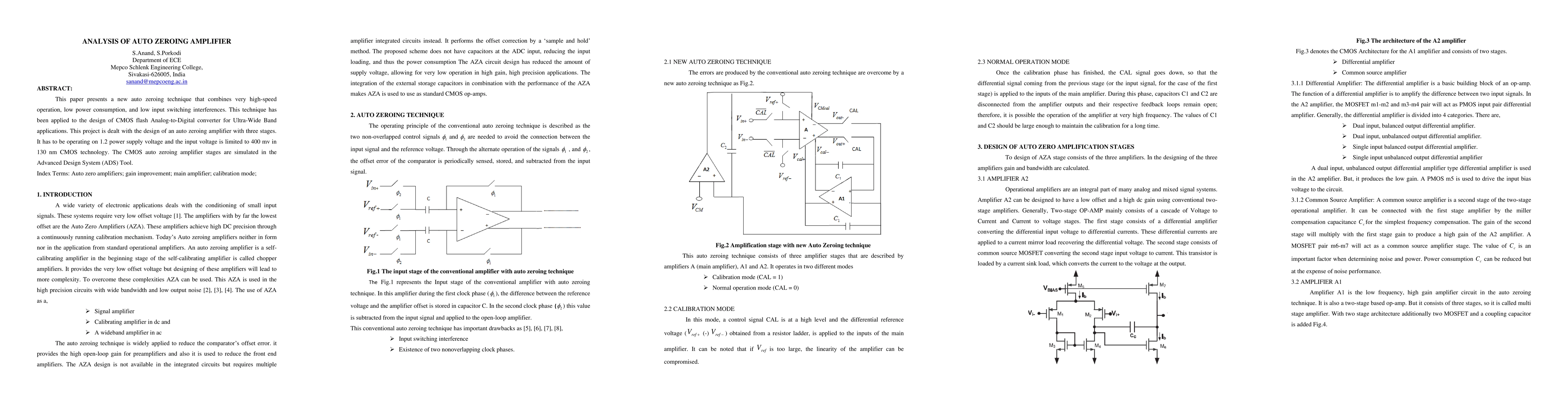
Abstract
This paper presents a new auto zeroing technique that combines very high-speed operation, low power consumption, and low input switching interferences. This technique has been applied to the design of CMOS flash Analog-to-Digital converter for Ultra-Wide Band applications. This project is dealt with the design of an auto zeroing amplifier with three stages. It has to be operating on 1.2 power supply voltage and the input voltage is limited to 400 mv in 130 nm CMOS technology. The CMOS auto zeroing amplifier stages are simulated in the Advanced Design System (ADS) Tool.
AI Key Findings
Get AI-generated insights about this paper's methodology, results, significance, and more — seven facets brought into focus.
Impact
Paper Details
Authors
PDF Preview
Key Terms
Citation Network
Current paper (gray), citations (green), references (blue)
Display is limited for performance on very large graphs.
Discussion 0