Publication
Metrics
AI Quick Summary
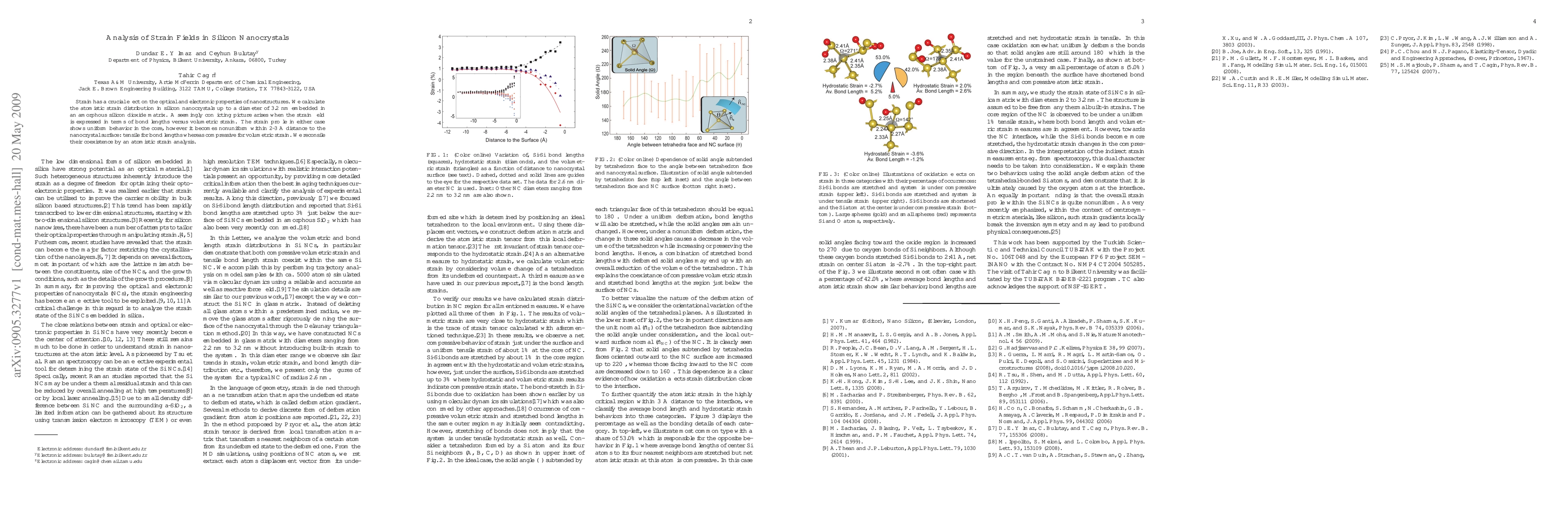
This research analyzes strain fields in silicon nanocrystals up to 3.2 nm in diameter within an amorphous silicon dioxide matrix. It finds conflicting yet coexisting strain behaviors: uniform tensile strain near bonds and compressive volumetric strain, resolved through atomistic strain analysis.
Paper Preview
Abstract
Strain has a crucial effect on the optical and electronic properties of nanostructures. We calculate the atomistic strain distribution in silicon nanocrystals up to a diameter of 3.2 nm embedded in an amorphous silicon dioxide matrix. A seemingly conflicting picture arises when the strain field is expressed in terms of bond lengths versus volumetric strain. The strain profile in either case shows uniform behavior in the core, however it becomes nonuniform within 2-3 \AA distance to the nanocrystal surface: tensile for bond lengths whereas compressive for volumetric strain. We reconsile their coexistence by an atomistic strain analysis.
AI Key Findings
Get AI-generated insights about this paper's methodology, results, significance, and more — seven facets brought into focus.
Impact
Paper Details
PDF Preview
Key Terms
Citation Network
Current paper (gray), citations (green), references (blue)
Display is limited for performance on very large graphs.
Discussion 0