Analytical electron microscopy analysis of insulating and metallic phases in nanostructured vanadium dioxide
Publication
Metrics
AI Quick Summary
This paper uses analytical electron microscopy to study vanadium dioxide (VO$_2$) nanostructures, identifying insulating and metallic phases through high-resolution imaging and electron energy-loss spectroscopy. It finds that structural inhomogeneities do not adversely affect the material's optical properties, highlighting its potential for nanophotonics and optoelectronics.
Paper Preview
Abstract
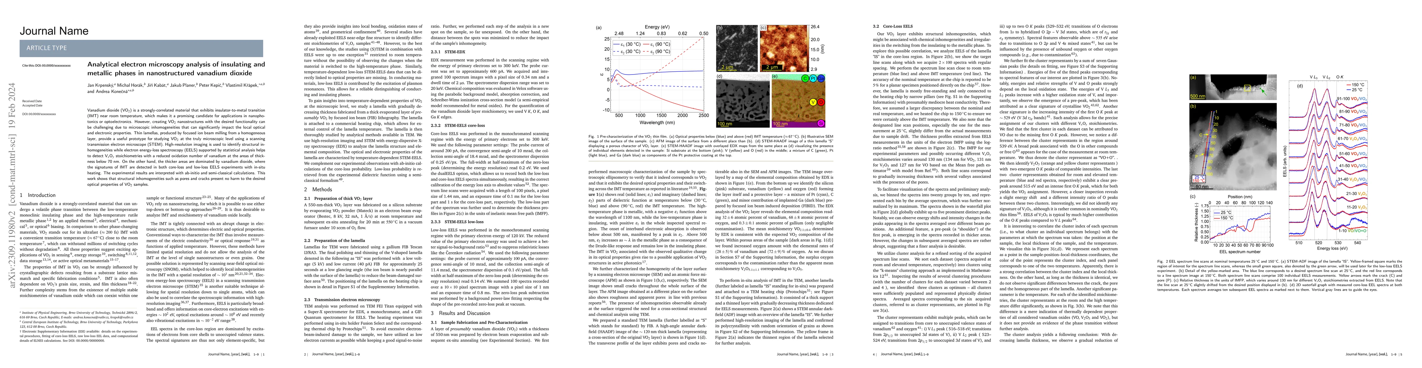
Vanadium dioxide (VO$_2$) is a strongly-correlated material that exhibits insulator-to-metal transition (IMT) near room temperature, which makes it a promising candidate for applications in nanophotonics or optoelectronics. However, creating VO$_2$ nanostructures with the desired functionality can be challenging due to microscopic inhomogeneities that can significantly impact the local optical and electronic properties. Thin lamellas, produced by focused ion beam milling from a homogeneous layer, provide a useful prototype for studying VO$_2$ at the truly microscopic level using a scanning transmission electron microscope (STEM). High-resolution imaging is used to identify structural inhomogeneities while electron energy-loss spectroscopy (EELS) supported by statistical analysis helps to detect V$_x$O$_y$ stoichiometries with a reduced oxidation number of vanadium at the areas of thickness below 70 nm. On the other hand, the thicker areas are dominated by vanadium dioxide, where the signatures of IMT are detected in both core-loss and low-loss EELS experiments with in-situ heating. The experimental results are interpreted with ab-initio and semi-classical calculations. This work shows that structural inhomogeneities such as pores and cracks present no harm to the desired optical properties of VO$_2$ samples.
AI Key Findings
Get AI-generated insights about this paper's methodology, results, significance, and more — seven facets brought into focus.
Impact
Paper Details
Authors
PDF Preview
Key Terms
Citation Network
Current paper (gray), citations (green), references (blue)
Display is limited for performance on very large graphs.
Discussion 0