01
MethodologyHow they did it
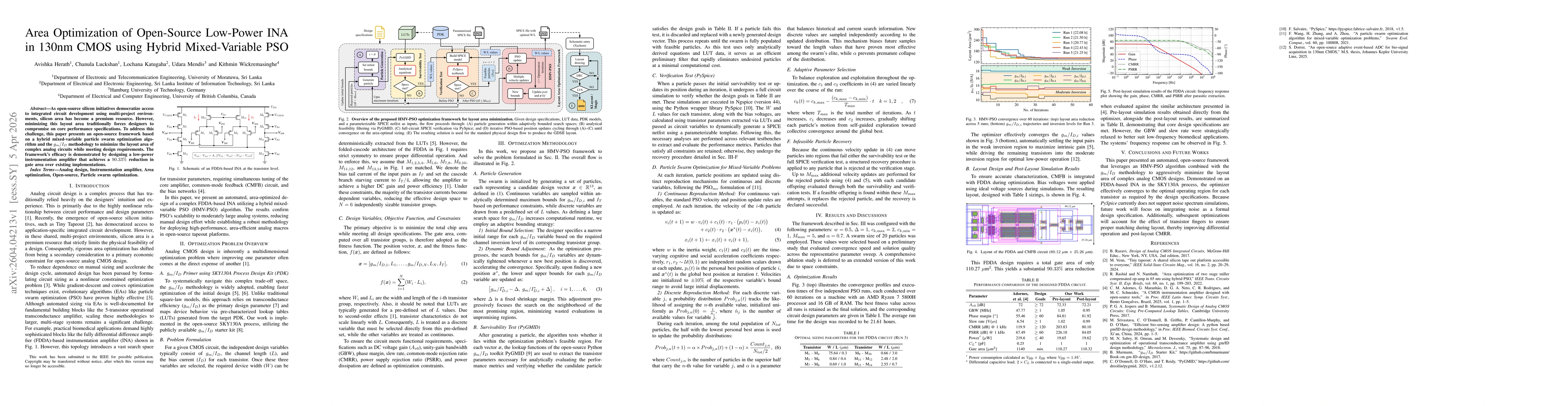
Hybrid mixed-variable particle swarm optimization combined with gm/ID lookup tables, analytical feasibility filtering via PyGMID, and full circuit verification using PySpice, applied to a 130nm CMOS FDDA-based instrumentation amplifier.
Discussion 0