Quick Summary:

This paper explores the use of direct bonded copper (DBC) substrates for creating high-power atom chips, highlighting benefits such as excellent adhesion, high thermal conductivity, and rapid fabrication. It presents two fabrication mask options and etching methods, determining optimal wire aspect ratios and thicknesses for magnetic trapping.

Summary

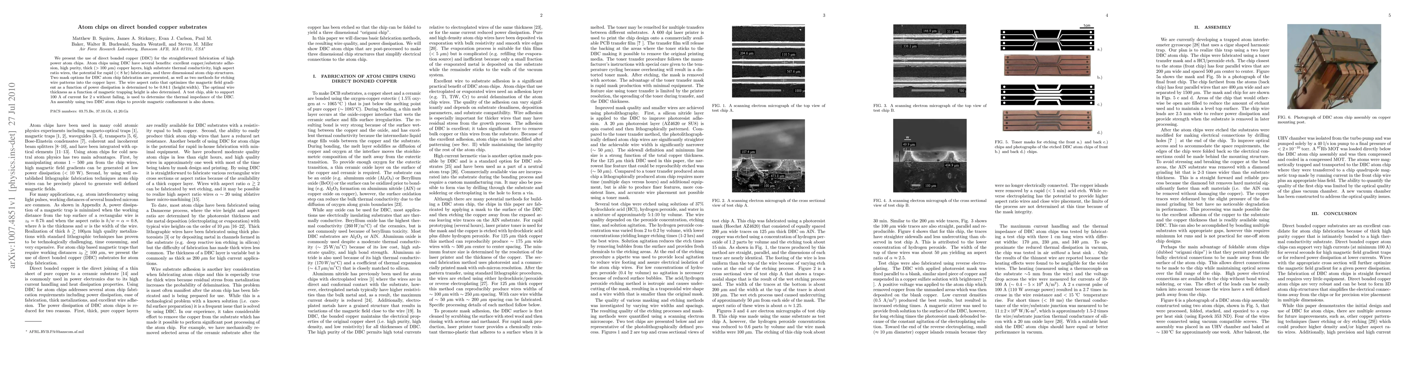
We present the use of direct bonded copper (DBC) for the straightforward fabrication of high power atom chips. Atom chips using DBC have several benefits: excellent copper/substrate adhesion, high purity, thick (> 100 microns) copper layers, high substrate thermal conductivity, high aspect ratio wires, the potential for rapid (< 8 hr) fabrication, and three dimensional atom chip structures. Two mask options for DBC atom chip fabrication are presented, as well as two methods for etching wire patterns into the copper layer. The wire aspect ratio that optimizes the magnetic field gradient as a function of power dissipation is determined to be 0.84:1 (height:width). The optimal wire thickness as a function of magnetic trapping height is also determined. A test chip, able to support 100 A of current for 2 s without failing, is used to determine the thermal impedance of the DBC. An assembly using two DBC atom chips to provide magnetic confinement is also shown.

AI Key Findings

Get AI-generated insights about this paper's methodology, results, and significance.

Paper Details

PDF Preview

Download PDF

Key Terms

wire (0.293)
chip (0.289)
atom (0.288)
fabrication (0.277)
substrate (0.212)
aspect (0.205)
height (0.201)
magnetic (0.154)
thermal (0.151)
determined (0.149)
ratio (0.143)
purity (0.141)
high (0.136)
hr (0.135)
optimizes (0.135)
thermal conductivity (0.133)
trapping (0.133)
options (0.131)
power (0.129)
assembly (0.129)

Citation Network

Current paper (gray), citations (green), references (blue)

Current Paper
Citations
References
Click to view
Title Authors Year Actions
Bose-Einstein-condensate source on an optical-grating-based atom chip for quantum sensor applications
R. Calviac, A. Rouxel, S. Charlot, D. Bourrier, A. Arnoult, A. Monmayrant, O. Gauthier-Lafaye, A. Gauguet, B. Allard
2024
View Paper
Review of Atom Chips for Absolute Gravity Sensors
Dezhao Li, Wenfeng He, Shengnan Shi, Bin Wu, Yuhua Xiao, Q. Lin, Long Li
2023
View Paper
Time-orbiting-potential chip trap for cold atoms
C. Sackett, J. Stickney
2023
View Paper
Trapping ultracold atoms in submicron period magnetic lattices
T. Tran, Yao Wang, I. Herrera, A. Balčytis, D. Nissen, M. Albrecht, Shannon Whitlock, A. Sidorov, P. Hannaford
2019
View Paper
A cylindrically symmetric magnetic trap for compact Bose-Einstein condensate atom interferometer gyroscopes.
R. Horne, C. Sackett
2017
View Paper
Ex vacuo atom chip Bose-Einstein condensate
M. Squires, S. Olson, B. Kasch, James A. Stickney, C. Erickson, J. Crow, E. Carlson, J. H. Burke
2016
View Paper
Chip-Scale Magnetic Source of Cold Atoms
Eric Imhof
2013
View Paper
Ac Zeeman Force With Ultracold Atoms
C. Fancher
2016
View Paper
Advanced Devices and Electronic Packaging for Harsh Environment
A. Elshabini, F. Barlow, Sharmin Islam, P. Wang
2013
View Paper

Comments (0)

This website uses cookies to ensure you get the best experience. Learn more