Publication
Metrics
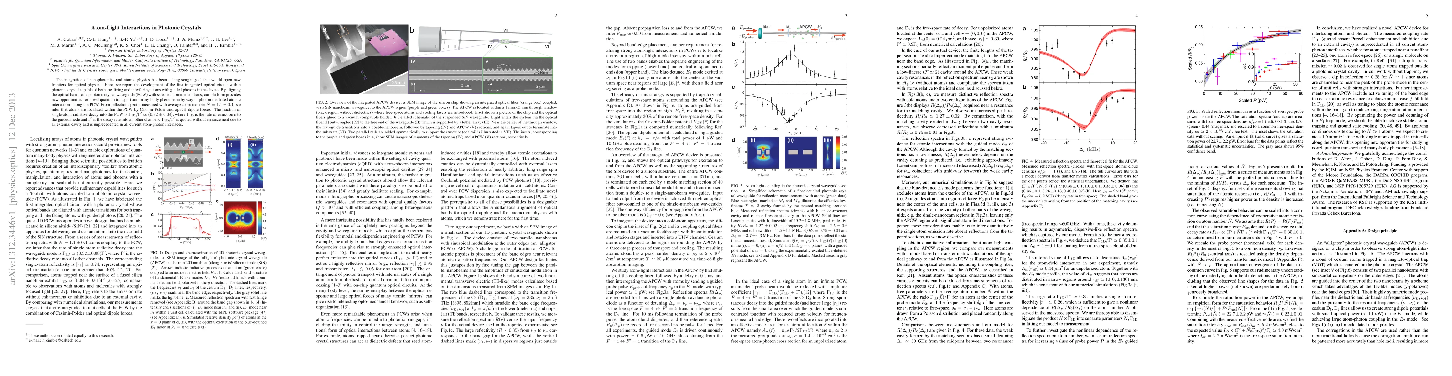
AI Quick Summary
This paper presents a novel photonic crystal circuit that interfaces atoms with guided photons, enabling photon-mediated atomic interactions. The platform achieves unprecedented localization and coupling of atoms within the photonic crystal waveguide, with a single-atom emission rate into the guided mode of 0.32±0.08 relative to all decay channels, showcasing significant potential for quantum transport and many-body phenomena.
Paper Preview
Abstract
The integration of nanophotonics and atomic physics has been a long-sought goal that would open new frontiers for optical physics. Here, we report the development of the first integrated optical circuit with a photonic crystal capable of both localizing and interfacing atoms with guided photons in the device. By aligning the optical bands of a photonic crystal waveguide (PCW) with selected atomic transitions, our platform provides new opportunities for novel quantum transport and many-body phenomena by way of photon-mediated atomic interactions along the PCW. From reflection spectra measured with average atom number N = 1.1$\pm$0.4, we infer that atoms are localized within the PCW by Casimir-Polder and optical dipole forces. The fraction of single-atom radiative decay into the PCW is $\Gamma_{\rm 1D}/\Gamma'$ = 0.32$\pm$0.08, where $\Gamma_{1D}$ is the rate of emission into the guided mode and $\Gamma'$ is the decay rate into all other channels. $\Gamma_{\rm 1D}/\Gamma'$ is quoted without enhancement due to an external cavity and is unprecedented in all current atom-photon interfaces.
AI Key Findings
Get AI-generated insights about this paper's methodology, results, significance, and more — seven facets brought into focus.
Impact
Paper Details
PDF Preview
Key Terms
Citation Network
Current paper (gray), citations (green), references (blue)
Display is limited for performance on very large graphs.
Discussion 0