Atomic and electronic structure of defects in hBN: enhancing single-defect functionalities
Publication
Metrics
AI Quick Summary
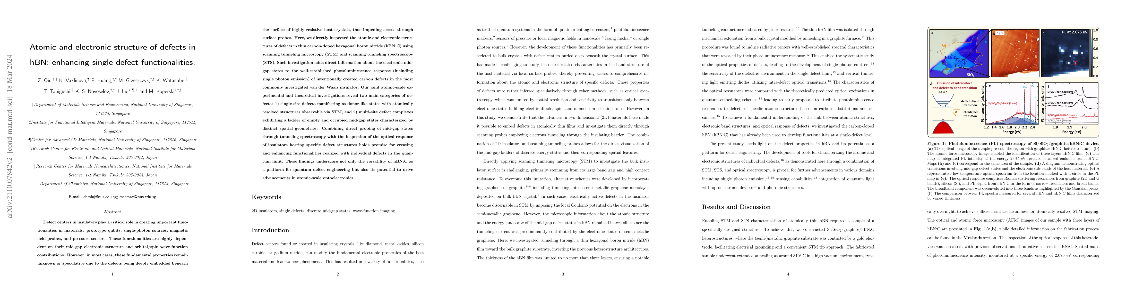
This paper utilizes scanning tunneling microscopy and spectroscopy to directly investigate the atomic and electronic structures of defects in carbon-doped hexagonal boron nitride (hBN:C). It identifies two defect categories: single-site donor-like defects and multi-site complexes with ladders of mid-gap states, revealing their potential for quantum functionalities and optoelectronics.
Paper Preview
Abstract
Defect centers in insulators play a critical role in creating important functionalities in materials: prototype qubits, single-photon sources, magnetic field probes, and pressure sensors. These functionalities are highly dependent on their mid-gap electronic structure and orbital/spin wave-function contributions. However, in most cases, these fundamental properties remain unknown or speculative due to the defects being deeply embedded beneath the surface of highly resistive host crystals, thus impeding access through surface probes. Here, we directly inspected the atomic and electronic structures of defects in thin carbon-doped hexagonal boron nitride (hBN:C) using scanning tunneling microscopy (STM) and scanning tunneling spectroscopy (STS). Such investigation adds direct information about the electronic mid-gap states to the well-established photoluminescence response (including single photon emission) of intentionally created carbon defects in the most commonly investigated van der Waals insulator. Our joint atomic-scale experimental and theoretical investigations reveal two main categories of defects: 1) single-site defects manifesting as donor-like states with atomically resolved structures observable via STM, and 2) multi-site defect complexes exhibiting a ladder of empty and occupied mid-gap states characterized by distinct spatial geometries. Combining direct probing of mid-gap states through tunneling spectroscopy with the inspection of the optical response of insulators hosting specific defect structures holds promise for creating and enhancing functionalities realized with individual defects in the quantum limit. These findings underscore not only the versatility of hBN:C as a platform for quantum defect engineering but also its potential to drive advancements in atomic-scale optoelectronics.
AI Key Findings
Get AI-generated insights about this paper's methodology, results, significance, and more — seven facets brought into focus.
Paper Details
Authors
PDF Preview
Key Terms
Citation Network
Current paper (gray), citations (green), references (blue)
Display is limited for performance on very large graphs.
Related Papers
No references found for this paper.
Discussion 0