Publication
Metrics
AI Quick Summary
This paper investigates how atomic vacancy defects affect the electronic properties of MoS$_2$ and WS$_2$ monolayers using a Slater-Koster tight-binding model. The study finds that these defects create localized states in the bandgap, potentially altering the electronic structure based on defect type and concentration.
Paper Preview
Abstract
The influence of atomic vacancy defects at different concentrations on electronic properties of MoS$_2$ and WS$_2$ monolayers is studied by means of Slater-Koster tight-binding model with non-orthogonal $sp^3d^5$ orbitals and including the spin-orbit coupling. The presence of vacancy defects induces localized states in the bandgap of pristine MoS$_2$ and WS$_2$, which have potential to modify the electronic structure of the systems, depending on the type and concentration of the defects. It is shown that although the contribution of metal (Mo or W) $d$ orbitals is dominant in the formation of midgap states, the sulphur $p$ and $d$ orbitals have also considerable contribution in the localized states, when metal defects are introduced. Our results suggest that Mo and W defects can turn the monolayers into p-type semiconductors, while the sulphur defects make the system a n-type semiconductor, in agreement with ab initio results and experimental observations.
AI Key Findings
Get AI-generated insights about this paper's methodology, results, significance, and more — seven facets brought into focus.
Impact
Paper Details
PDF Preview
Key Terms
Citation Network
Current paper (gray), citations (green), references (blue)
Display is limited for performance on very large graphs.
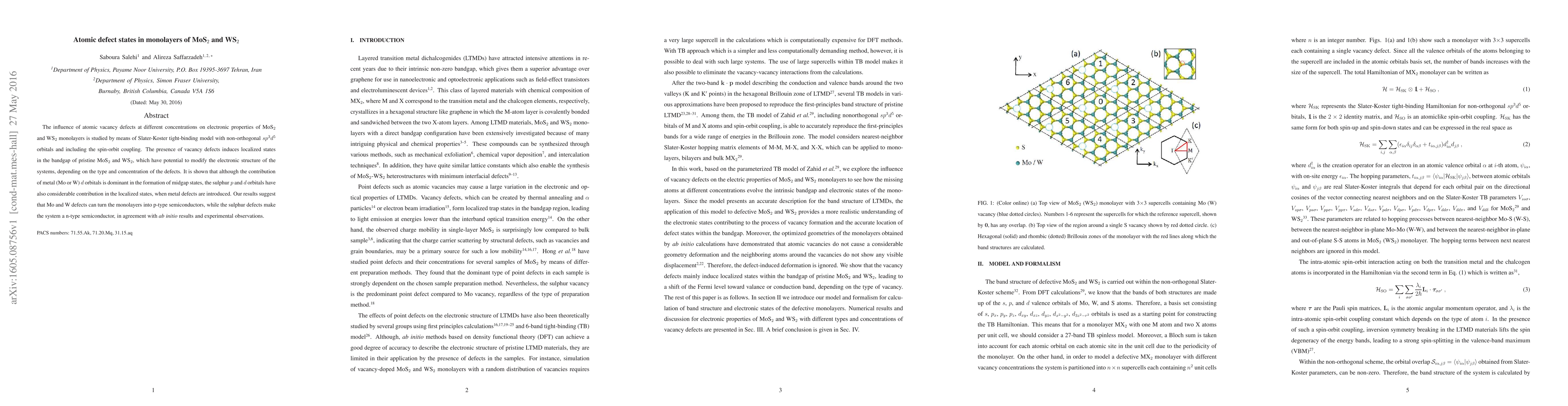
Discussion 0