Summary
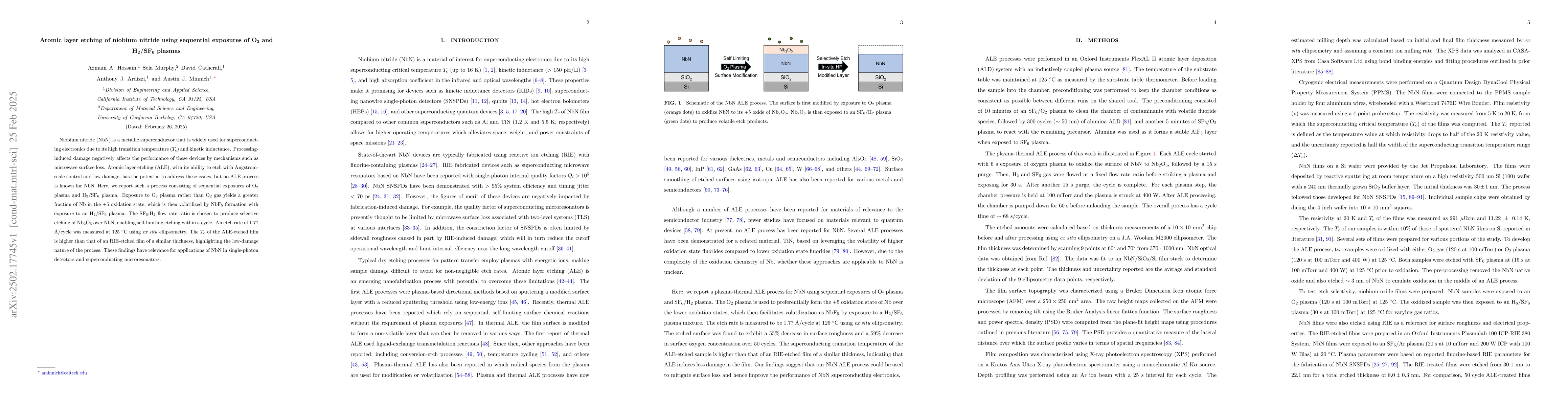
Niobium nitride (NbN) is a metallic superconductor that is widely used for superconducting electronics due to its high transition temperature ($T_c$) and kinetic inductance. Processing-induced damage negatively affects the performance of these devices by mechanisms such as microwave surface loss. Atomic layer etching (ALE), with its ability to etch with Angstrom-scale control and low damage, has the potential to address these issues, but no ALE process is known for NbN. Here, we report such a process consisting of sequential exposures of O$_2$ plasma and H$_2$/SF$_6$ plasma. Exposure to O$_2$ plasma rather than O$_2$ gas yields a greater fraction of Nb in the +5 oxidation state, which is then volatilized by NbF$_5$ formation with exposure to an H$_2$/SF$_6$ plasma. The SF$_6$:H$_2$ flow rate ratio is chosen to produce selective etching of Nb$_2$O$_5$ over NbN, enabling self-limiting etching within a cycle. An etch rate of 1.77 \r{A}/cycle was measured at 125 $^\circ$C using ex-situ ellipsometry. The $T_c$ of the ALE-etched film is higher than that of an RIE-etched film of a similar thickness, highlighting the low-damage nature of the process. These findings have relevance for applications of NbN in single-photon detectors and superconducting microresonators.
AI Key Findings
Generated Jun 11, 2025
Methodology
The research introduces an Atomic Layer Etching (ALE) process for niobium nitride (NbN) using sequential exposures of O2 plasma and H2/SF6 plasma, achieving Angstrom-scale control and low damage.
Key Results
- Development of an ALE process for NbN using O2 and H2/SF6 plasmas.
- O2 plasma exposure increases Nb in the +5 oxidation state, which is then volatilized by NbF5 formation with H2/SF6 plasma.
- Selective etching of Nb2O5 over NbN achieved with an appropriate SF6:H2 ratio, enabling self-limiting etching.
- An etch rate of 1.77 Å/cycle measured at 125 °C using ex-situ ellipsometry.
- ALE-etched NbN film retains a higher Tc compared to RIE-etched film of similar thickness, demonstrating low-damage etching.
Significance
This research is significant for applications of NbN in superconducting electronics, such as single-photon detectors and microresonators, by providing a low-damage etching process that can mitigate processing-induced damage.
Technical Contribution
The introduction of a novel ALE process for niobium nitride, utilizing O2 and H2/SF6 plasmas for precise and low-damage etching.
Novelty
This work presents the first reported ALE process for niobium nitride, offering Angstrom-scale control and low damage, which is crucial for superconducting electronics applications.
Limitations
- The study does not explore the scalability of the ALE process for large-area NbN etching.
- Potential long-term effects of the ALE process on NbN properties are not discussed.
Future Work
- Investigate the scalability of the ALE process for industrial applications.
- Examine the long-term stability and reliability of ALE-etched NbN films.
Paper Details
PDF Preview
Citation Network
Current paper (gray), citations (green), references (blue)
Display is limited for performance on very large graphs.
Similar Papers
Found 4 papersDirectional atomic layer etching of MgO-doped lithium niobate using sequential exposures of H$_2$ and SF$_6$ plasma
Alireza Marandi, Ryoto Sekine, Austin J. Minnich et al.
Isotropic plasma-thermal atomic layer etching of superconducting TiN films using sequential exposures of molecular oxygen and SF$_6/$H$_2$ plasma
Haozhe Wang, Austin J. Minnich, Azmain A. Hossain et al.
Atomic layer etching of SiO$_2$ using sequential exposures of Al(CH$_3$)$_3$ and H$_2$/SF$_6$ plasma
David Catherall, Azmain Hossain, Austin Minnich
Atomic layer etching of SiO$_2$ using sequential SF$_6$ gas and Ar plasma
Jun Peng, Rakshith Venugopal, Robert Blick et al.
No citations found for this paper.
Comments (0)