A novel approach combining scanning tunneling microscopy and spectroscopy to study single-electron tunneling in silicon quantum dots
Publication
Metrics
AI Quick Summary
Researchers demonstrate atomic-scale control of tunnel coupling in single-electron transistors, overcoming challenges in scalable solid-state quantum computing.
Quick Answers
What is "Atomic-scale Control of Tunnel Coupling" about?
Researchers demonstrate atomic-scale control of tunnel coupling in single-electron transistors, overcoming challenges in scalable solid-state quantum computing.
What methodology did the authors use?
A novel approach combining scanning tunneling microscopy and spectroscopy to study single-electron tunneling in silicon quantum dots More in Methodology →
What are the key results?
Observation of Coulomb blockade oscillations in a Si:P delta-doped layer — Measurement of the electric field and capacitance between the electrodes More in Key Results →
Why is this work significant?
This research demonstrates the potential for single-electron tunneling to be used as a scalable and reliable method for quantum computing More in Significance →
What are the main limitations?
Limited by the small size of the Si:P delta-doped layer — Sensitive to environmental factors such as temperature and humidity More in Limitations →
Abstract
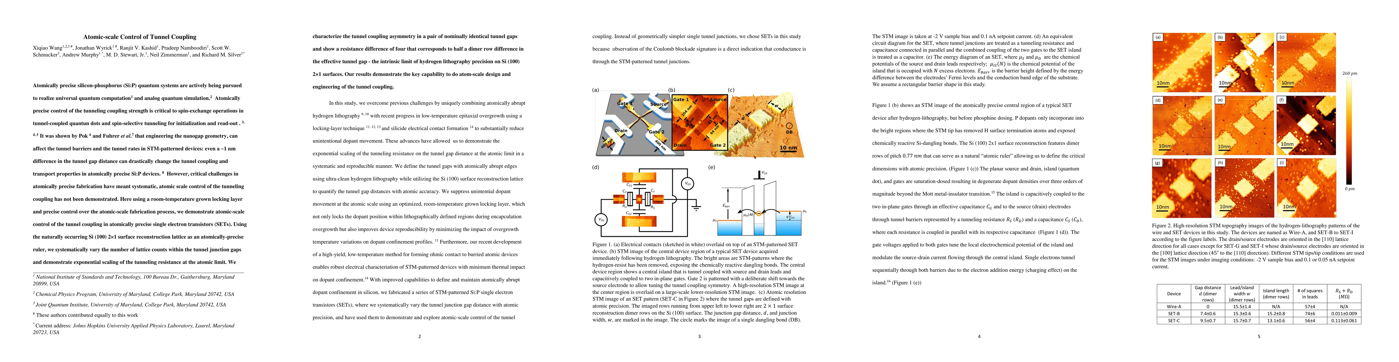
Atomically precise donor-based quantum devices are a promising candidate for scalable solid-state quantum computing. Atomically precise design and implementation of the tunnel coupling in these devices is essential to realize gate-tunable exchange coupling, and electron spin initialization and readout. Current efforts in atomically precise lithography have enabled deterministic placement of single dopant atoms into the Si lattice with sub-nm precision. However, critical challenges in atomically precise fabrication have meant systematic, atomic-scale control of the tunneling coupling has not been demonstrated. Here using a room-temperature grown locking layer and precise control over the entire atomic-scale fabrication process, we demonstrate atomic-scale control of the tunnel coupling in atomically precise single-electron transistors (SETs). Using the naturally occurring Si (100) 2x1 surface reconstruction lattice as an atomically-precise ruler, we systematically vary the number of lattice counts within the tunnel junction gaps and demonstrate exponential scaling of the tunneling resistance at the atomic limit. Using low-temperature transport measurements, we characterize the tunnel coupling asymmetry in a pair of nominally identical tunnel gaps that results from atomic-scale variation in the tunnel junction and show a resistance difference of four that corresponds to half a dimer row pitch difference in the effective tunnel gap distances - the intrinsic limit of hydrogen lithography precision on Si (100) 2x1 surfaces. Our results demonstrate the key capability to do atom-scale design and engineering of the tunnel coupling necessary for solid-state quantum computing and analog quantum simulation.
Key Findings, in focus
Seven facets of this paper, analysed and brought into focus by AI.
This research demonstrates the potential for single-electron tunneling to be used as a scalable and reliable method for quantum computing
- Observation of Coulomb blockade oscillations in a Si:P delta-doped layer
- Measurement of the electric field and capacitance between the electrodes
- Determination of the energy levels of the quantum dot
This research demonstrates the potential for single-electron tunneling to be used as a scalable and reliable method for quantum computing
The development of a new theoretical model for single-electron tunneling in silicon quantum dots
This work presents a novel approach to studying single-electron tunneling in silicon quantum dots using scanning tunneling microscopy and spectroscopy
- Limited by the small size of the Si:P delta-doped layer
- Sensitive to environmental factors such as temperature and humidity
- Investigating the use of other semiconductor materials for quantum computing
- Developing more robust methods for measuring the electric field and capacitance between electrodes
Impact
Paper Details
PDF Preview
Key Terms
Citation Network
Current paper (gray), citations (green), references (blue)
Display is limited for performance on very large graphs.
Discussion 0