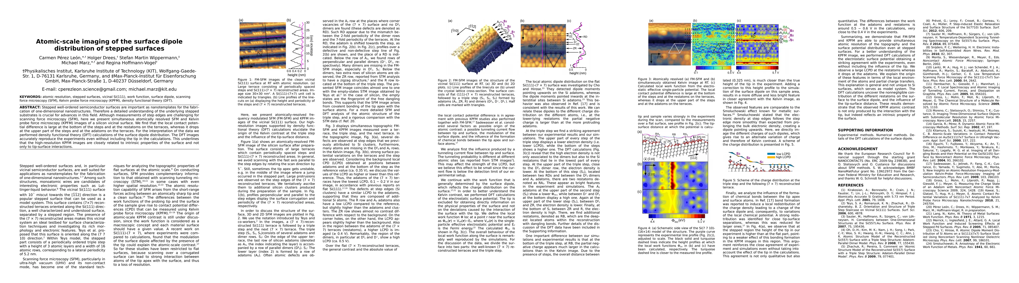
This paper presents atomically resolved scanning force microscopy and Kelvin probe force microscopy images of a silicon vicinal surface, revealing non-homogeneous local contact potential differences due to differences in surface dipole distribution at step edges, explained by a Smoluchowski-type effect. Density functional theory calculations confirm these findings, highlighting intrinsic surface properties rather than tip-surface interactions.
Stepped well-ordered semiconductor surfaces are important as nanotemplates for the fabrication of one-dimensional nanostructures which are candidates of intriguing electronic properties. Therefore a detailed understanding of the underlying stepped substrates is crucial for advances in this field. Although measurements of step edges are challenging for scanning force microscopy (SFM), here we present for the first time simultaneous atomically resolved SFM and Kelvin probe force microscopy (KPFM) images of a silicon vicinal surface. We find that the local contact potential difference is not homogeneous over all silicon atoms, contrary to the common understanding of the work function. For the interpretation of the data we performed density functional theory (DFT) calculations. We explain the atomic-scale electronic features by differences in the surface dipole distribution caused by a Smoluchowski-type effect. E.g., at step edges the partial negative charge is larger at the lower-lying atoms closer to the bulk than at the atoms more protruding towards the vacuum. This is the first manifestation of such type of effect on a semiconductor surface. The DFT images accurately reproduce the experiments even without including the tip in the calculations. This underlines that the high-resolution KPFM images indeed show the intrinsic properties of the surface and not only tip-surface interactions.
Get AI-generated insights about this paper's methodology, results, and significance.
Current paper (gray), citations (green), references (blue)
Title | Authors | Year | Actions |
---|---|---|---|
Effective removal of global tilt from atomically-resolved topography images of vicinal surfaces with narrow terraces.
|
A. Aladyshkin, A. N. Chaika, V. N. Semenov, A. Ionov, S. Bozhko
|
2024
|
View Paper |
Single-dopant band bending fluctuations in
<mml:math xmlns:mml="http://www.w3.org/1998/Math/MathML"><mml:msub><mml:mrow><mml:mi>MoSe</mml:mi></mml:mrow><mml:mn>2</mml:mn></mml:msub></mml:math>
measured with electrostatic force microscopy
|
M. Cowie, Rikke Plougmann, Z. Schumacher, P. Grütter
|
2022
|
View Paper |
Local work function on graphene nanoribbons
|
Daniel Rothhardt, Amina Kimouche, Tillmann Klamroth, Regina Hoffmann-Vogel
|
2022
|
View Paper |
Comment on “Experimental Evidence for a New Two-Dimensional Honeycomb Phase of Silicon: A Missing Link in the Chemistry and Physics of Silicon Surfaces?”
|
R. Zhachuk, J. Coutinho
|
2021
|
View Paper |
Theory for Potential of Zero Charge and Capacitance on Metals with Nanocorrugated Steps
|
G. Mishra, R. Kant
|
2021
|
View Paper |
Anomalous Scaling of Aeolian Sand Transport Reveals Coupling to Bed Rheology.
|
K. Tholen, T. Pähtz, S. Kamath, E. Parteli, K. Kroy
|
2021
|
View Paper |
Electrostatic forces above graphene nanoribbons and edges interpreted as partly hydrogen-free.
|
Sebastian Schneider, R. Hoffmann-Vogel
|
2020
|
View Paper |
Electrocatalysis
|
Electrocatalysis
|
2020
|
View Paper |
Film Thickness of Pb Islands on the Si(111) Surface.
|
Th Späth, M. Popp, R. Hoffmann-Vogel
|
2020
|
View Paper |
Imaging the surface potential at the steps on the rutile TiO2(110) surface by Kelvin probe force microscopy
|
Masato Miyazaki, Huang Wen, Quanzhen Zhang, Y. Adachi, J. Brndiar, I. Štich, Y. Li, Y. Sugawara
|
2019
|
View Paper |
Determination of Specific Electrocatalytic Sites in the Oxidation of Small Molecules on Crystalline Metal Surfaces
|
M. Farias, J. Feliu
|
2019
|
View Paper |
Magnification Effects in Scanning Tunneling Microscopy: the Role of Surface Radicals
|
R. Zhachuk, J. Coutinho
|
2019
|
View Paper |
Electromigration and the structure of metallic nanocontacts
|
R. Hoffmann-Vogel
|
2017
|
View Paper |
Near-equilibrium measurement of quantum size effects using Kelvin probe force microscopy.
|
Th Späth, M. Popp, C. Pérez León, M. Marz, R. Hoffmann-Vogel
|
2017
|
View Paper |
Structure and local charging of electromigrated Au nanocontacts
|
Daniel Arnold, M. Marz, Sebastian Schneider, R. Hoffmann-Vogel
|
2017
|
View Paper |
Band gap manipulation and physical properties of preferred orientation CuO thin films with nano wheatear array
|
Yue Chen, Lin Zhang, Haotian Zhang, Kehua Zhong, Guiying Zhao, Guilin Chen, Yingbin Lin, Shuiyuan Chen, Zhigao Huang
|
2018
|
View Paper |
Imaging Static Charge Distributions: A Comprehensive KPFM Theory
|
P. Rahe, H. Söngen
|
2018
|
View Paper |
Comments (0)