Quick Summary:

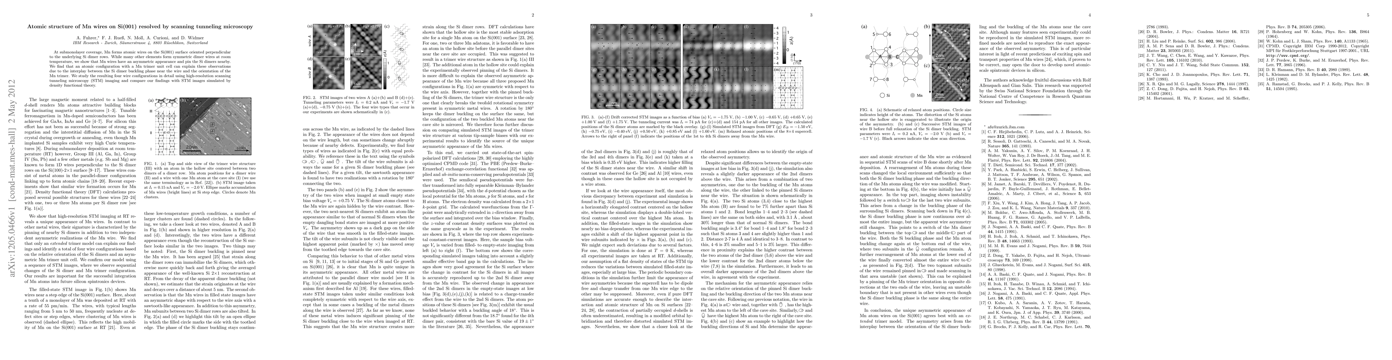
The study reveals that Mn wires on Si(001) surface form asymmetric structures, pinning nearby Si dimers, and proposes a Mn trimer unit cell to explain these features. High-resolution scanning tunneling microscopy (STM) and density functional theory (DFT) simulations corroborate four distinct wire configurations.

Summary

At submonolayer coverage, Mn forms atomic wires on the Si(001) surface oriented perpendicular to the underlying Si dimer rows. While many other elements form symmetric dimer wires at room temperature, we show that Mn wires have an asymmetric appearance and pin the Si dimers nearby. We find that an atomic configuration with a Mn trimer unit cell can explain these observations due to the interplay between the Si dimer buckling phase near the wire and the orientation of the Mn trimer. We study the resulting four wire configurations in detail using high-resolution scanning tunneling microscopy (STM) imaging and compare our findings with STM images simulated by density functional theory.

AI Key Findings

Get AI-generated insights about this paper's methodology, results, and significance.

Paper Details

PDF Preview

Download PDF

Key Terms

mn (0.364)
si (0.334)
wire (0.278)
atomic (0.197)
unit cell (0.160)
using high (0.154)
room temperature (0.154)
room (0.148)
coverage (0.147)
scanning (0.146)
tunneling (0.142)
functional theory (0.142)
perpendicular (0.141)
microscopy (0.137)
orientation (0.137)
density functional (0.136)
appearance (0.136)
nearby (0.134)
interplay (0.133)
oriented (0.133)
Title Authors Year Actions
Mn doped Sr/Si(111)-(3×2) HCC surfaces: antiferromagnetic semiconductors for spintronic applications.
Jun-Shuai Chai, Jian-Tao Wang, Li-fang Xu
2020
View Paper
Atomic Scale Design, Structure and Stability of Quantum Nanowires Located on Epitaxial Interfaces and Free‐Standing in Space
M. Michailov
2019
View Paper
Atomic layer doping of Mn magnetic impurities from surface chains at a Ge/Si hetero-interface.
K. Murata, C. Kirkham, S. Tsubomatsu, Takashi Kanazawa, K. Nitta, Y. Terada, T. Uruga, K. Nittoh, D. Bowler, K. Miki
2017
View Paper
Magnetism in Mn Nanowires and Clusters as {\delta}-doped Layers in Group IV Semiconductors (Si, Ge)
K. R. Simov, P. Glans, C. Jenkins, M. Liberati, P. R. D. O. M. Science, Engineering, U. Virginia, 395 McCormick Road, Charlottesville, VA 22901, U. A. L. Source, L. B. N. Laboratory, Berkeley, California
2017
View Paper
Monatomic metal nanowires: Rupture kinetics and mean lifetime
M. Michailov, D. Kashchiev
2015
View Paper
Magnetic property of transition metal-Si atomic line on silicon Σ3 grain boundary: A theoretical study
Y. Li, Shuxia Guo, Zhongquan Ma, G. Qu, T. Shi, X. Gong, Q. Xia, S. Wei
2014
View Paper
Towards a Mn-Co surface alloy: Scanning Tunneling Microscopy (STM) study of Co adsorption on Si(100) and its interaction with Mn wires
Gopalakrishnan Ramalingam, P. Reinke
2014
View Paper
Confinement and integration of magnetic impurities in silicon
F. Rueß, M. Kazzi, L. Czornomaz, P. Mensch, M. Hopstaken, A. Fuhrer
2013
View Paper
Magnetism in Mn-nanowires and -clusters as δ-doped layers in group IV semiconductors
K. R. Simov, P. Glans, C. A. Jenkins, M. Liberati, P. Reinke
2018
View Paper
Bi and Mn nanostructures on the Si(001) surface
C. Kirkham
2014
View Paper

Comments (0)

This website uses cookies to ensure you get the best experience. Learn more