Atomic Structure of Self-Buffered BaZr(S,Se)$_3$ Epitaxial Thin Film Interfaces
Publication
Metrics
AI Quick Summary
This study elucidates the atomic structure of self-buffered BaZr(S,Se)$_3$ thin films on LaAlO$_3$ substrates using advanced microscopy, revealing an epitaxial buffer layer that accommodates lattice mismatch and transitions to perovskite structure, aiding in the development of optoelectronic devices.
Paper Preview
Abstract
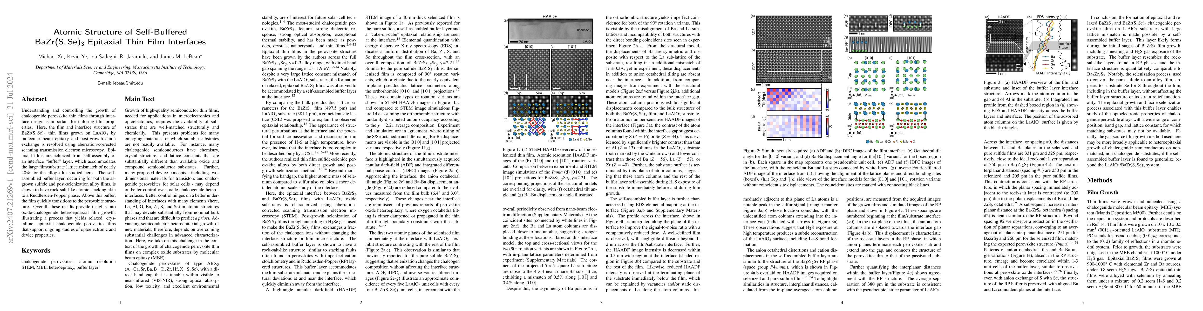
Understanding and controlling the growth of chalcogenide perovskite thin films through interface design is important for tailoring film properties. Here, the film and interface structure of BaZr(S,Se)$_3$ thin films grown on LaAlO$_3$ by molecular beam epitaxy and post-growth anion exchange is resolved using aberration-corrected scanning transmission electron microscopy. Epitaxial films are achieved from self-assembly of an interface ``buffer'' layer, which accommodates the large film/substrate lattice mismatch of nearly 40\% for the alloy film studied here. The self-assembled buffer layer, occurring for both the as-grown sulfide and post-selenization alloy films, is shown to have rock-salt-like atomic stacking akin to a Ruddlesden-Popper phase. Above this buffer, the film quickly transitions to the perovskite structure. Overall, these results provide insights into oxide-chalcogenide heteroepitaxial film growth, illustrating a process that yields relaxed, crystalline, epitaxial chalcogenide perovskite films that support ongoing studies of optoelectronic and device properties.
AI Key Findings
Get AI-generated insights about this paper's methodology, results, significance, and more — seven facets brought into focus.
Impact
Authors
PDF Preview
Citation Network
Current paper (gray), citations (green), references (blue)
Display is limited for performance on very large graphs.
Discussion 0