Publication
Metrics
AI Quick Summary
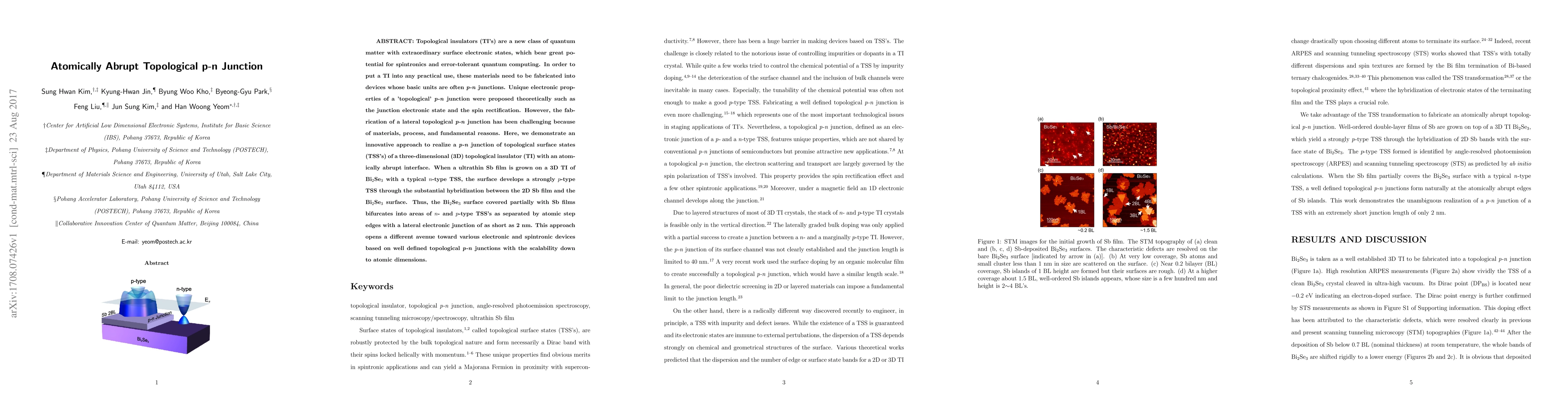
This paper demonstrates the fabrication of an atomically abrupt topological p-n junction by growing ultrathin Sb films on a 3D topological insulator Bi2Se3, resulting in a lateral junction with electronic states as short as 2 nm. This innovation paves the way for scalable spintronic and quantum computing devices based on well-defined topological surface states.
Paper Preview
Abstract
Topological insulators (TI's) are a new class of quantum matter with extraordinary surface electronic states, which bear great potential for spintronics and error-tolerant quantum computing. In order to put a TI into any practical use, these materials need to be fabricated into devices whose basic units are often p-n junctions. Unique electronic properties of a 'topological' p-n junction were proposed theoretically such as the junction electronic state and the spin rectification. However, the fabrication of a lateral topological p-n junction has been challenging because of materials, process, and fundamental reasons. Here, we demonstrate an innovative approach to realize a p-n junction of topological surface states (TSS's) of a three-dimensional (3D) topological insulator (TI) with an atomically abrupt interface. When a ultrathin Sb film is grown on a 3D TI of Bi2Se3 with a typical n-type TSS, the surface develops a strongly p-type TSS through the substantial hybridization between the 2D Sb film and the Bi2Se3 surface. Thus, the Bi2Se3 surface covered partially with Sb films bifurcates into areas of n- and p-type TSS's as separated by atomic step edges with a lateral electronic junction of as short as 2 nm. This approach opens a different avenue toward various electronic and spintronic devices based on well defined topological p-n junctions with the scalability down to atomic dimensions
AI Key Findings
Get AI-generated insights about this paper's methodology, results, significance, and more — seven facets brought into focus.
Impact
Paper Details
PDF Preview
Key Terms
Citation Network
Current paper (gray), citations (green), references (blue)
Display is limited for performance on very large graphs.
Discussion 0