The study employs nano-confinement techniques with graphene and hBN as capping layers to control the growth of TMD monolayers. It utilizes precursor intercalation, substitution reactions, and defect engineering to achieve patterned and large-scale TMD synthesis.
Atomically-precise synthesis and simultaneous integration of 2D transition metal dichalcogenides enabled by nano-confinement
Publication
Metrics
Quick Answers
What methodology did the authors use?
The study employs nano-confinement techniques with graphene and hBN as capping layers to control the growth of TMD monolayers. It utilizes precursor intercalation, substitution reactions, and defect engineering to achieve patterned and large-scale TMD synthesis. More in Methodology →
What are the key results?
Selective intercalation of NbSe2 precursors into MoS2/SiO2 interface enables one-side substitution — Defects in capping layers act as additional intercalation paths for precursor surface diffusion More in Key Results →
Why is this work significant?
This research enables precise synthesis of tailored TMD monolayers with controlled morphology and electronic properties, crucial for next-generation 2D electronics and integrated circuits More in Significance →
What are the main limitations?
Limited scalability of defect engineering approach — Potential surface contamination from SiO2 substrates More in Limitations →
Abstract
Two-dimensional (2D) materials, such as graphene, transition metal dichalcogenides (TMDs), and hBN, exhibit intriguing properties that are sensitive to their atomic-scale structures and can be further enriched through van der Waals (vdW) integration. However, the precise synthesis and clean integration of 2D materials remain challenging. Here, using graphene or hBN as a vdW capping layer, we create a nano-confined environment that directs the growth kinetics of 2D TMDs (e.g., NbSe2 and MoS2), enabling precise formation of TMD monolayers with tailored morphologies, from isolated monolayer domains to large-scale continuous films and intrinsically-patterned rings. Moreover, Janus S-Mo-Se monolayers are synthesized with atomic precision via vdW-protected bottom-plane chalcogen substitution. Importantly, our approach simultaneously produces ultraclean vdW interfaces. This in situ encapsulation reliably preserves air-sensitive materials, as evidenced by the enhanced superconductivity of nano-confined NbSe2 monolayers. Altogether, our study establishes a versatile platform for the controlled synthesis and integration of 2D TMDs for advanced applications.
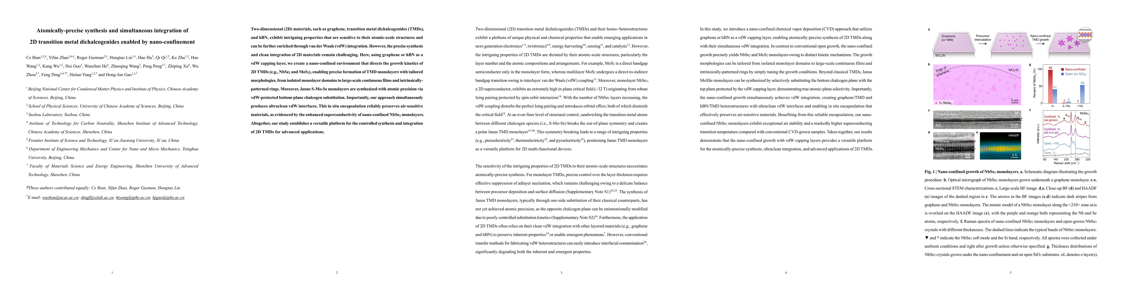
Key Findings, in focus
Seven facets of this paper, analysed and brought into focus by AI.
This research enables precise synthesis of tailored TMD monolayers with controlled morphology and electronic properties, crucial for next-generation 2D electronics and integrated circuits
- Selective intercalation of NbSe2 precursors into MoS2/SiO2 interface enables one-side substitution
- Defects in capping layers act as additional intercalation paths for precursor surface diffusion
- Four-regime phase diagram maps growth morphology under nano-confinement
This research enables precise synthesis of tailored TMD monolayers with controlled morphology and electronic properties, crucial for next-generation 2D electronics and integrated circuits
Development of a four-regime phase diagram for predicting and controlling nano-confinement growth morphology
First demonstration of defect-mediated precursor intercalation for patterned TMD synthesis and large-scale monolayer fabrication
- Limited scalability of defect engineering approach
- Potential surface contamination from SiO2 substrates
- Exploring other TMD materials with similar techniques
- Optimizing defect density for better intercalation control
Discussion 0