Scanning Electron Microscopy (SEM) is indispensable for characterizing the
microstructure of thin films during perovskite solar cell fabrication. Accurate
identification and quantification of lead iodide and perovskite phases are
critical because residual lead iodide strongly influences crystallization
pathways and defect formation, while the morphology of perovskite grains
governs carrier transport and device stability. Yet current SEM image analysis
is still largely manual, limiting throughput and consistency. Here, we present
an automated deep learning-based framework for SEM image segmentation that
enables precise and efficient identification of lead iodide, perovskite and
defect domains across diverse morphologies. Built upon an improved YOLOv8x
architecture, our model named PerovSegNet incorporates two novel modules: (i)
Adaptive Shuffle Dilated Convolution Block, which enhances multi-scale and
fine-grained feature extraction through group convolutions and channel mixing;
and (ii) Separable Adaptive Downsampling module, which jointly preserves
fine-scale textures and large-scale structures for more robust boundary
recognition. Trained on an augmented dataset of 10,994 SEM images, PerovSegNet
achieves a mean Average Precision of 87.25% with 265.4 Giga Floating Point
Operations, outperforming the baseline YOLOv8x-seg by 4.08%, while reducing
model size and computational load by 24.43% and 25.22%, respectively. Beyond
segmentation, the framework provides quantitative grain-level metrics, such as
lead iodide/perovskite area and count, which can serve as reliable indicators
of crystallization efficiency and microstructural quality. These capabilities
establish PerovSegNet as a scalable tool for real-time process monitoring and
data-driven optimization of perovskite thin-film fabrication.The source code is
available at:https://github.com/wlyyj/PerovSegNet/tree/master.
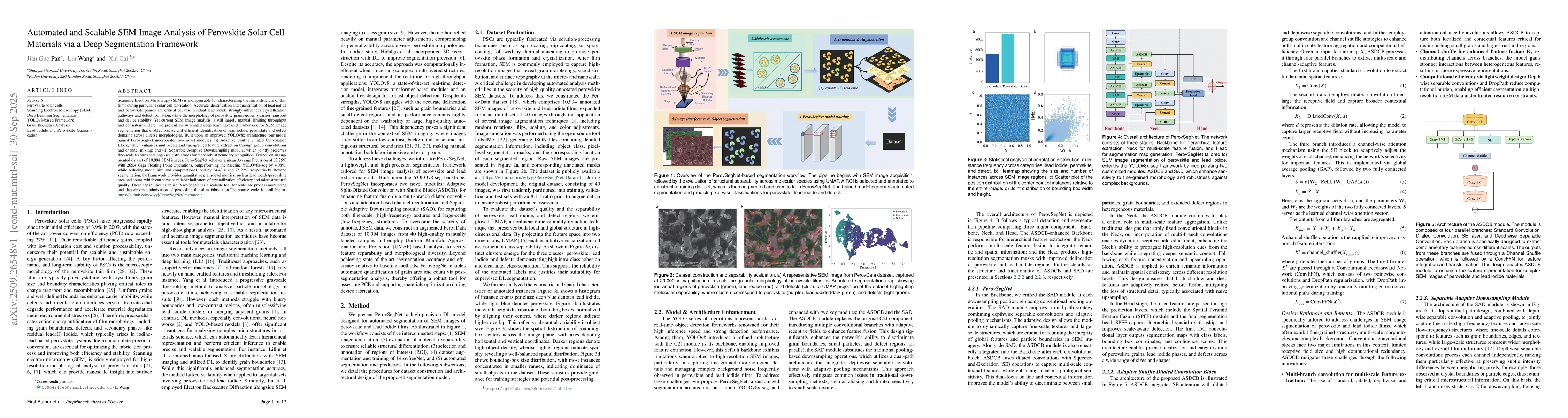
Discussion 0