Publication
Metrics
AI Quick Summary
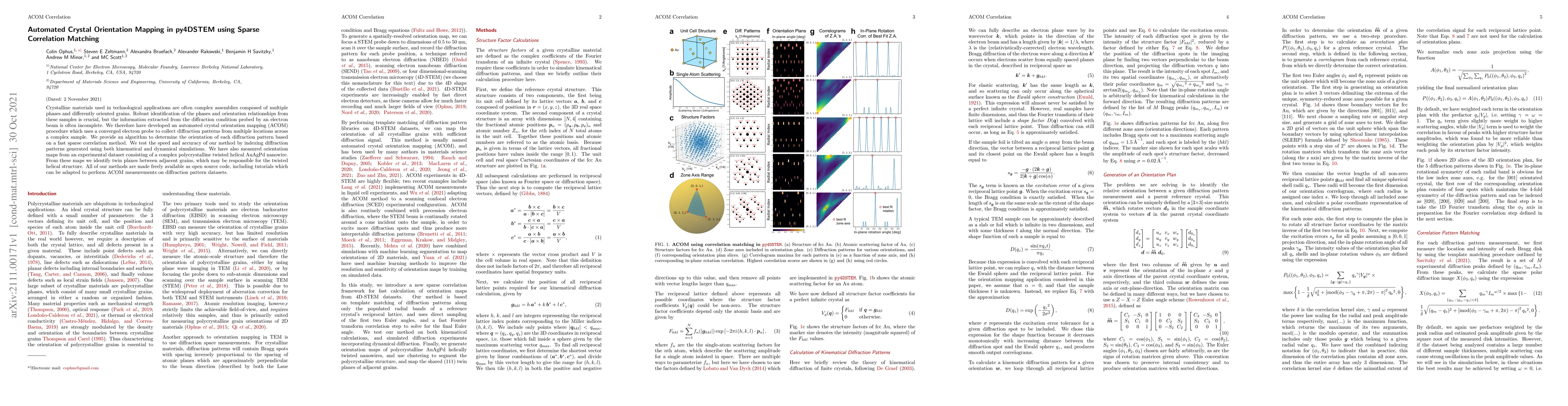
This paper presents an automated crystal orientation mapping (ACOM) method using sparse correlation matching in py4DSTEM to identify phases and orientation relationships in complex polycrystalline materials. The proposed algorithm efficiently determines the orientation of diffraction patterns, validated through simulations and an experimental nanowire, revealing twin planes that contribute to its helical structure.
Paper Preview
Abstract
Crystalline materials used in technological applications are often complex assemblies composed of multiple phases and differently oriented grains. Robust identification of the phases and orientation relationships from these samples is crucial, but the information extracted from the diffraction condition probed by an electron beam is often incomplete. We therefore have developed an automated crystal orientation mapping (ACOM) procedure which uses a converged electron probe to collect diffraction patterns from multiple locations across a complex sample. We provide an algorithm to determine the orientation of each diffraction pattern based on a fast sparse correlation method. We test the speed and accuracy of our method by indexing diffraction patterns generated using both kinematical and dynamical simulations. We have also measured orientation maps from an experimental dataset consisting of a complex polycrystalline twisted helical AuAgPd nanowire. From these maps we identify twin planes between adjacent grains, which may be responsible for the twisted helical structure. All of our methods are made freely available as open source code, including tutorials which can be easily adapted to perform ACOM measurements on diffraction pattern datasets.
AI Key Findings
Get AI-generated insights about this paper's methodology, results, significance, and more — seven facets brought into focus.
Impact
Paper Details
Authors
PDF Preview
Key Terms
Citation Network
Current paper (gray), citations (green), references (blue)
Display is limited for performance on very large graphs.
Discussion 0