The research introduces ballast charges, induced charges on a screening layer beneath semiconductor spin qubits, to counteract charge noise caused by fluctuating electromagnetic environments.
Publication
Metrics
AI Quick Summary
The study introduces ballast charges in semiconductor spin qubits to mitigate electromagnetic noise, significantly improving dephasing times by a factor of 4 to 6. This method employs an additional screening layer to counter electromagnetic fluctuations, thus enhancing qubit stability for quantum computing applications.
Quick Answers
What is "Ballast charges for semiconductor spin qubits" about?
The study introduces ballast charges in semiconductor spin qubits to mitigate electromagnetic noise, significantly improving dephasing times by a factor of 4 to 6. This method employs an additional screening layer to counter electromagnetic fluctuations, thus enhancing qubit stability for quantum computing applications.
What methodology did the authors use?
The research introduces ballast charges, induced charges on a screening layer beneath semiconductor spin qubits, to counteract charge noise caused by fluctuating electromagnetic environments. More in Methodology →
What are the key results?
Simulations show that the dephasing time of a spin qubit in a Si/SiGe device increases by a factor of 4 to 6 on average when using ballast charges. — Double quantum well structures, Ge spikes in SiQW, and patterned screening layers are discussed as potential physical implementations. More in Key Results →
Why is this work significant?
This approach significantly reduces the power spectral density associated with fluctuations from two-level systems, enhancing the stability and performance of semiconductor spin qubits for quantum computing applications. More in Significance →
What are the main limitations?
Creating additional screening layers might require significant fabrication development and challenging patterning processes. — Ballast charges could increase the energy required for gate operations on qubits due to their counteractive role against intentional changes in gate voltages. More in Limitations →
Abstract
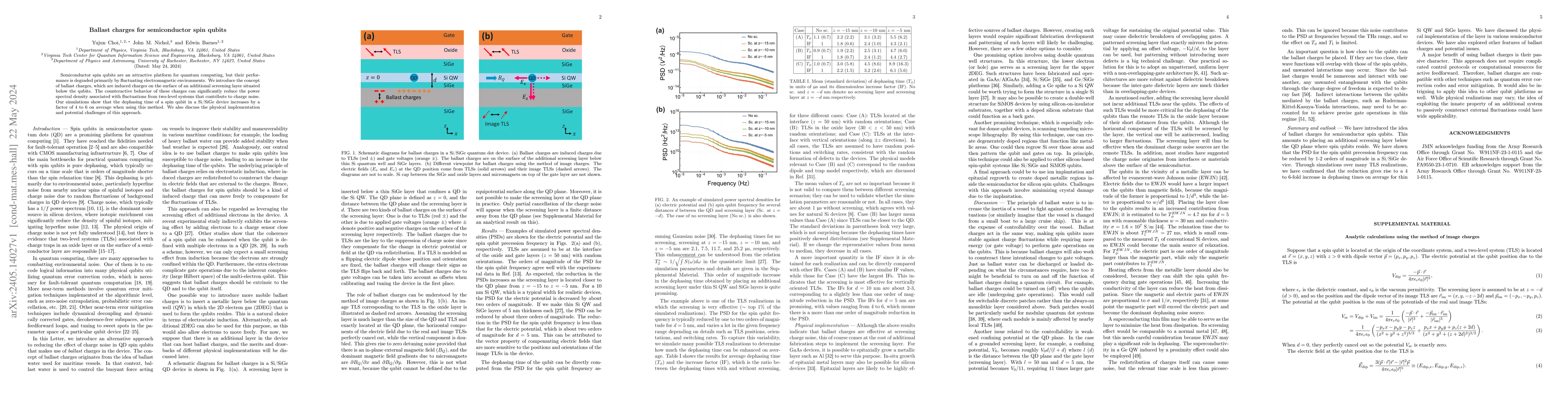
Semiconductor spin qubits are an attractive platform for quantum computing, but their performance is degraded primarily by fluctuating electromagnetic environments. We introduce the concept of ballast charges, which are induced charges on the surface of an additional screening layer situated below the qubits. The counteractive behavior of these charges can significantly reduce the power spectral density associated with fluctuations from two-level systems that contribute to charge noise. Our simulations show that the dephasing time of a spin qubit in a Si/SiGe device increases by a factor of 4 to 6 on average when using this method. We also discuss the physical implementation and potential challenges of this approach.
Key Findings, in focus
Seven facets of this paper, analysed and brought into focus by AI.
This approach significantly reduces the power spectral density associated with fluctuations from two-level systems, enhancing the stability and performance of semiconductor spin qubits for quantum computing applications.
- Simulations show that the dephasing time of a spin qubit in a Si/SiGe device increases by a factor of 4 to 6 on average when using ballast charges.
- Double quantum well structures, Ge spikes in SiQW, and patterned screening layers are discussed as potential physical implementations.
- The passive nature of ballast charges makes them compatible with other techniques like quantum error correction codes and error mitigation.
This approach significantly reduces the power spectral density associated with fluctuations from two-level systems, enhancing the stability and performance of semiconductor spin qubits for quantum computing applications.
The concept of ballast charges for semiconductor spin qubits, which involves an additional screening layer to reduce charge noise and increase qubit coherence times.
This work introduces a novel method to mitigate charge noise in semiconductor spin qubits by exploiting the inertia of ballast charges against external fluctuations, offering passive protection without complex control protocols.
- Creating additional screening layers might require significant fabrication development and challenging patterning processes.
- Ballast charges could increase the energy required for gate operations on qubits due to their counteractive role against intentional changes in gate voltages.
- Exploration of other semiconductor devices for implementing ballast charges, such as SiMOS devices using silicon-on-insulator substrates.
- Investigation of scanning tunneling microscopy lithography for creating degenerately doped regions that function as metallic areas.
Impact
Paper Details
Authors
PDF Preview
Key Terms
Citation Network
Current paper (gray), citations (green), references (blue)
Display is limited for performance on very large graphs.
Discussion 0