Publication
Metrics
AI Quick Summary
This paper presents a novel method for engineering the band structure of 2D materials using patterned dielectric superlattices, achieving high mobility and smaller wavelength patterns by integrating surface dielectric patterning with van der Waals materials. The technique demonstrates replica Dirac cones in graphene and fractal Hofstadter spectra under large magnetic fields, showcasing dynamic tunability and versatility.
Paper Preview
Abstract
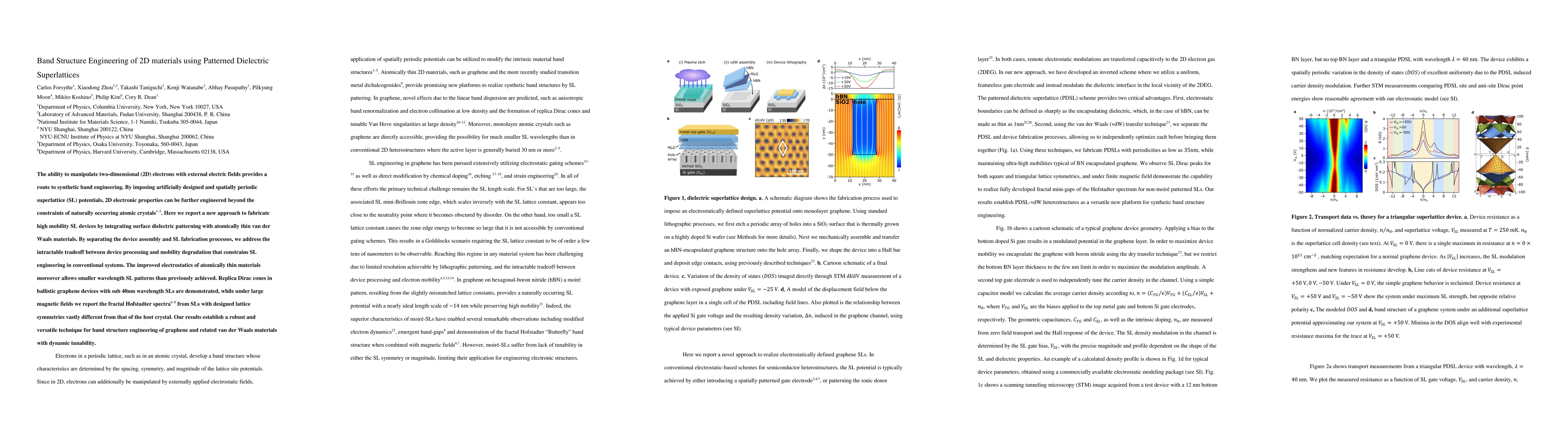
The ability to manipulate two-dimensional (2D) electrons with external electric fields provides a route to synthetic band engineering. By imposing artificially designed and spatially periodic superlattice (SL) potentials, 2D electronic properties can be further engineered beyond the constraints of naturally occurring atomic crystals. Here we report a new approach to fabricate high mobility SL devices by integrating surface dielectric patterning with atomically thin van der Waals materials. By separating the device assembly and SL fabrication processes, we address the intractable tradeoff between device processing and mobility degradation that constrains SL engineering in conventional systems. The improved electrostatics of atomically thin materials moreover allows smaller wavelength SL patterns than previously achieved. Replica Dirac cones in ballistic graphene devices with sub 40nm wavelength SLs are demonstrated, while under large magnetic fields we report the fractal Hofstadter spectra from SLs with designed lattice symmetries vastly different from that of the host crystal. Our results establish a robust and versatile technique for band structure engineering of graphene and related van der Waals materials with dynamic tunability.
AI Key Findings
Get AI-generated insights about this paper's methodology, results, significance, and more — seven facets brought into focus.
Impact
Paper Details
PDF Preview
Key Terms
Citation Network
Current paper (gray), citations (green), references (blue)
Display is limited for performance on very large graphs.
Discussion 0